


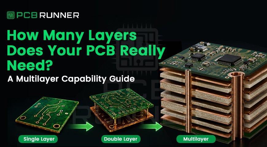
How Many Layers Does Your PCB Really Need? A Multilayer Capability Guide
Objective This guide gives design engineers and procurement teams a practical way to answer one recurring question: how many layers

Objective This guide gives design engineers and procurement teams a practical way to answer one recurring question: how many layers
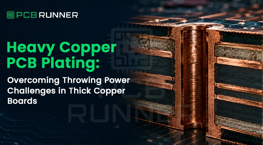
Objective This blog post explains why heavy copper PCB plating becomes harder as copper weight climbs, what throwing power actually
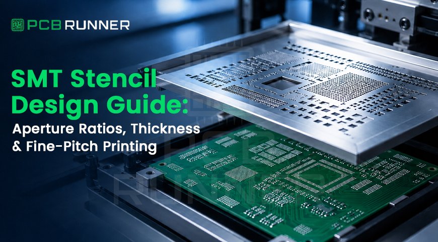
Objective: Give SMT engineers and PCB assembly buyers a technically accurate, practical guide to stencil aperture ratios, thickness selection, and
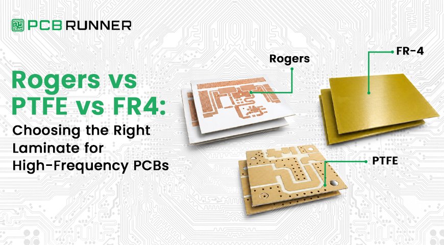
Objective: Give RF and hardware engineers a clear, technically grounded way to choose between FR4, Rogers, and PTFE laminates for
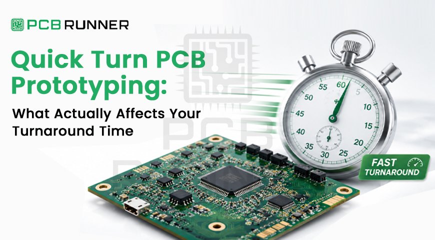
Objective To explain what affects quick-turn PCB prototyping timelines and how businesses can avoid common delays to get prototypes faster.
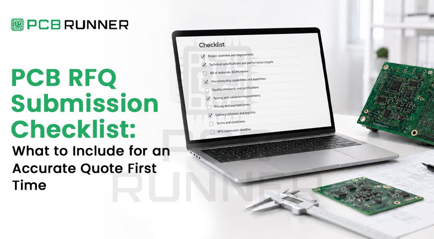
Objective Give engineers and buyers a practical, no-fluff checklist for submitting a PCB RFQ that gets an accurate quote on
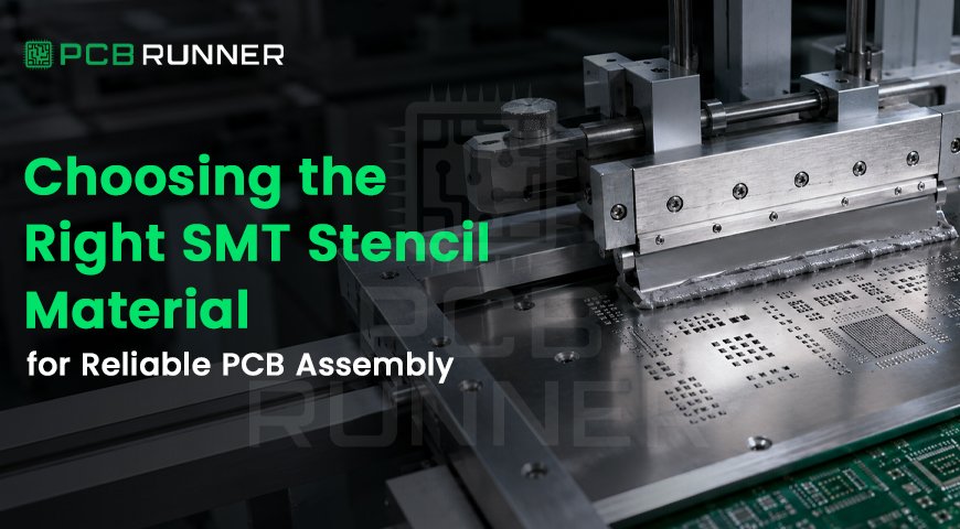
Objective Explain how SMT stencil material choice affects solder paste deposition and first-pass yield, and give buyers a practical way
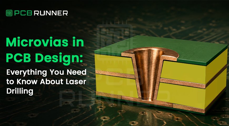
Objective Explain how microvias in PCB design work, why laser drilling replaced mechanical drilling for HDI boards, and what to
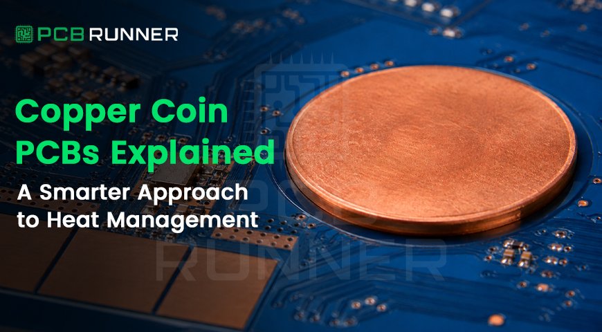
Objective Explain how Copper Coin PCB technology moves heat out of high-power boards, where it beats standard thermal management methods,
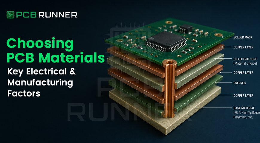
Objective To help engineers and buyers understand what actually drives PCB Material Selection, so board specs match the application instead
Fill out our comprehensive online PCB & Assembly specification form and receive instant pricing via email.
 +44 203 2397011
 sales@pcbrunner.com
Have any advanced capability PCB design? Upload your files for our review and get a personalized quote from our Sales Engineer Executive via email.
+44 203 2397011sales@pcbrunner.com