


SMT Stencils
Precision Solder Paste Printing for SMT Assembly
Many SMT assembly defects can begin during solder paste printing. Bridging, insufficient solder, tombstoning and inconsistent joints can result from incorrect paste volume or poor transfer through the stencil aperture.
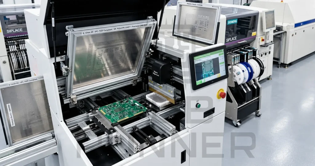
PCB Runner uses SMT stencils as part of the PCB SMT assembly process to achieve controlled and repeatable solder paste deposition before component placement. We support specified aperture and stencil thickness requirements, including step-up and step-down stencils where different paste volumes are required across the PCB
Send your Gerber and paste layer files across for a same-day quote, with an aperture review included.
Capability Chart
| Parameter | Capability |
|---|---|
| Cutting Method | Laser cut, standard on every order |
| Material | Stainless steel |
| Standard Thickness | 0.1mm, 0.12mm, 0.15mm |
| Minimum Aperture | Down to 0.15mm for fine-pitch and 01005 parts |
| Frame Options | Framed and frameless |
| Step Stencils | Multi-level thickness for mixed-height boards |
| Coating | Nano-coating available for improved paste release |
| Aperture Design Standard | IPC-7525 area ratio guidelines |
| Turnaround | Prototype stencils typically 1–2 days from approval |
Non-standard thickness or aperture size? Flag it before the paste layer is finalised. It’s a quick fix on file, a rework once the stencil’s cut.
Services Offered
Prototype Assembly
SMT stencils are used for controlled solder paste printing during prototype PCB assembly, helping achieve the required paste deposition for component pads before placement.
Production Assembly
For production PCB assembly, the specified stencil is used to provide repeatable solder paste deposition across production runs and support consistent SMT processing.
Step-Up and Step-Down Stencils
We support step-up and step-down stencils where different areas of the PCB require different solder paste volumes. Stencil thickness and aperture requirements are defined according to the component and assembly requirements.
Why Choose PCB Runner
Industries We Support
Consumer Electronics
Fine-pitch BGAs next to mixed 0201/0402 parts
Telecommunications
Dense RF modules with tight, mixed-pitch layouts
Medical Devices
Small-footprint boards with strict joint reliability
Automotive
High-volume sensor and control boards on continuous lines
Industrial Electronics
Mixed-height boards combining through-hole and SMT
Frequently Asked Questions
Laser cutting holds straighter aperture walls, which means more consistent paste release on fine-pitch parts. Etching struggles to control wall quality at small aperture sizes.
Every layer is checked against IPC-7525 before cutting. Anything likely to cause bridging or weak transfer gets flagged first.
Stencil thickness depends on the aperture dimensions and required solder paste volume. For rectangular apertures, the area ratio is calculated as (L × W) ÷ [2 × (L + W) × T], where T is stencil thickness. Final thickness should be selected according to the assembly requirements.
Yes. Small SMT parts next to taller components get different paste zones instead of one compromised setting across the board.
Yes. One file set for both removes a common cause of mismatch between what's printed and what's placed.
Gerber files with the paste layer included. A BOM helps if you want component-specific aperture review.
Both. Framed stencils are built for repeat use, and we support ongoing smt assembly UK-wide, not just one-off orders.



