High Density Interconnect PCB
High Density Interconnect PCB from HDI PCB Manufacturer
HDI PCB manufacturer PCB Runner is offering high-quality High-Density Interconnect PCB for the fast-moving electronic industry. HDI boards are one of the fastest growing technologies in PCBs. It is in your interests to start using the HDI PCB service from PCB Runner, as most likely, your competitors are already using them.

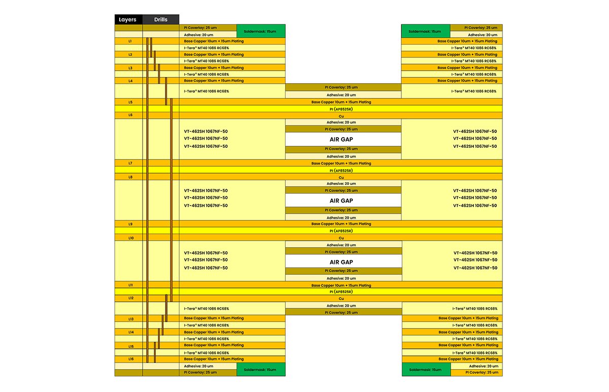
You need High Density Interconnect PCBs as they provide a new way of achieving more room on your board to make them more efficient, allowing for higher speeds and higher frequency operations. HDI boards offer higher circuit density, and the HDI PCB design incorporates much finer lines and spaces as compared to those on conventional PCBs. High Density Interconnect PCBs incorporate features such as blind and buried vias along with microvias with diameters equal to or less than 6 mils.
With more than a decade of HDI PCB manufacture and assembly experience, PCB Runner is offering high quality High Density Interconnect pcb services such as:
- Design
- Prototype
- Fabrication
Types of Advance PCB Boards
- Through vias from top-most layer to the bottom-most layer
- Blind vias between a surface layer and two or more HDI layers
- Buried vias between two or more inner HDI layers
- Passive substrates with no electrical connection
- Coreless construction using layer pairs
- Alternate coreless construction with layer pairs
HDI Board Key Advantages
Why to choose PCB design
Using HDI PCB design, you can reduce the overall dimensions and weight of your products, while enhancing their electrical performance. Several industries are already using such advanced PCB boards including 4G network communications, digital cameras, laptop computers, touch-screen devices, mobile phones, and medical devices.
Contact HDI PCB manufacturer PCB Runner today, and take advantage of the HDI PCB services we offer.
Technology with a Consumer Focus
As an HDI PCB manufacturer, we offer advanced technology with a focus on consumers. For instance, our via-in-pad process for our HDI boards offers more on fewer layers. Using HDI PCB technology, manufacturers of video cameras have reduced their footprint to make them fit in the palm of your hand. Mobile phones and computers have become lighter and faster, thanks to the HDI board technology they follow.
Therefore, if you want your products to be physically smaller, weigh less, and do more, we are available to help. Contact PCB Runner today, and we will help you with our specialty equipment and HDI PCB service to use smaller components and thinner materials, so that you can shrink the size of your products while expanding your technology and speed with a better quality.
HDI PCB Service
- Special Material and Lamination
- Contact Imagery & Laser Direct Imaging (LDI)
- Laser Drilling Technology
- Via-in-Pad Processing
- Filled Vias
- Cost-Effective HDI
HDI PCB Fabrication
Contact Us
We use Semiconductor Class 100 clean rooms for processing HDI designs for circuit board prototypes. This allows us to image finer lines, spacing, and finer annular rings. Although we use contact imagery, for still finer lines we use laser direct imaging or LDI. We use the latest in technology at PCB Runner HDI production facilities to produce such advance PCB boards.
We also use advanced technologies such as via-in-pads, and filled vias. Using our service, you can rest assured of achieving cost-effective HDI PCBs for your products.


