


Multilayer PCB Capabilities Built for Complex, High-Density Designs
As routing density, power distribution and signal-integrity requirements increase, multilayer construction often becomes the most practical way to achieve the required performance within the available board area. But adding layers also introduces tighter requirements for stackup design, layer registration, via structures, lamination and controlled impedance.
PCB Runner manufactures multilayer PCBs for prototypes through production requirements. Before fabrication, our CAM engineers review the manufacturing data, stackup and drill information to identify potential manufacturability issues with layer construction, drilling and other fabrication requirements before production begins.
Capability Chart
| Capability | Specification |
|---|---|
| Layer Count | 4 to 32+ layers |
| Board Thickness | 0.2mm to 6.0mm |
| Minimum Trace/Space | 3/3 mil |
| Minimum Via Size | 0.1mm laser drilled |
| Via Types | Through-hole, blind, buried, microvia |
| Impedance Tolerance | ±10% (tighter on request) |
| Base Materials | FR-4, high-Tg FR-4, Rogers, polyimide |
| Copper Weight | 0.5oz to 6oz |
| Surface Finish | ENIG, HASL, immersion silver, OSP |
| Max Panel Size | 24" x 18" |
These are the specs our shop runs on a regular basis. If your project sits outside any of these numbers, call us before you lock the design. It is easier to adjust a stackup on paper than after boards are already in production.
Multilayer PCB Manufacturing Services Offered by PCB Runner
A multilayer PCB board is only as good as the process behind it. Layer registration, dielectric consistency, and drill accuracy all have to hold together across the entire stack, not just on the outer layers.
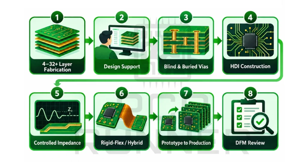
Multilayer PCB Fabrication
We build boards from 4 layers up to 32 or more. Registration between layers is checked at each press cycle, since even a small shift becomes a real problem once you are dealing with a dozen layers or more.
Multilayer PCB Design Support
Before a design goes to fabrication, our engineers review the stackup, layer sequencing, and copper balance. Most issues we catch at this stage are avoidable, and catching them here costs nothing compared to catching them after the boards are built.
Blind and Buried Via Manufacturing
Blind and buried vias let a design route through internal layers without eating up surface space. We drill both types to the tolerances dense boards actually need, not just to a spec sheet minimum.
HDI Multilayer Construction
High-density interconnect construction packs more circuitry into less board area. This comes up most often on wearables, compact consumer electronics, and computing hardware where every millimeter of board space is accounted for.
Controlled Impedance Stackups
RF circuits, high-speed digital lines, and mixed-signal designs all depend on the impedance staying where the design intended it to be. We build stackups around that requirement rather than treating it as an afterthought.
Rigid-Flex and Hybrid Multilayer Boards
Some designs need a flexible section built into an otherwise rigid multilayer structure. We run enough of these to have the process down, so it is not treated as a special one-off job.
Prototype and Production Scaling
Five prototype boards and five thousand production boards go through the same inspection steps here. Volume changes the schedule. It does not change what gets checked.
Design for Manufacturability (DFM) Review
Every multilayer order gets a DFM pass before fabrication. Stackup errors, drill file mismatches, and copper balance problems get caught and resolved on our end first.
Why Choose PCB Runner as Your Multilayer PCB Manufacturer
A lower quote does not mean much if the boards come back with registration problems or failed impedance tests. What actually matters is the process behind the number.
Engineering Review
Broad Layer Count Range
Material Flexibility
Fast Turnaround
Single Source Multilayer PCB
Direct Line to Engineering
- Engineering Review on Every Order: A CAM engineer looks at every file before production starts. If something is unclear, we ask instead of guessing at what you meant.
- Broad Layer Count Range: A simple 4-layer board and a dense 30-plus layer build both go through the same level of scrutiny here. Neither one gets treated as the easy job or the exception.
- Material Flexibility: Standard FR-4 covers a lot of designs, but not all of them. When a project needs high-Tg material or a specialty laminate like Rogers, we work with those options directly instead of pushing every job onto the same substrate.
- Fast Turnaround Without Skipping Steps: Same-day quotes and quick prototype turns are available, and the inspection process stays the same regardless of the deadline. Speed does not mean a shortcut through quality control.
- Single Source Multilayer PCB Supplier: Fabrication, drilling, plating, and testing all happen under one roof at PCB Runner. That cuts down on the handoffs where mistakes tend to slip in, and it usually shortens the lead time too.
- Direct Line to Engineering: Questions about your board go to the people who actually reviewed your files, not to a support queue that has to forward them along.
Quality & Inspection
Multilayer boards hide their problems better than simple ones. Once a board is pressed, the inner layers are sealed inside it. You cannot look at a finished board and confirm the internal routing is correct, which is exactly why inspection has to happen throughout production, not just at the final step.
Automated Optical Inspection (AOI)
Every panel is scanned for shorts, opens, and copper defects before it moves to the next stage. A defect caught here does not get built into the rest of the board.
Flying Probe and Electrical Testing
Each board is electrically tested against the original net list. This step catches wiring errors that would never show up on a visual inspection.
X-Ray Inspection
Blind vias, buried vias, and internal layer registration are invisible once the board is pressed together. X-ray lets us verify all three without cutting the board apart.
IPC Class 2 and Class 3 Compliance
Our processes follow IPC-6012 standards, with Class 3 available for applications where a board failure is not an option worth considering.
Documentation and Traceability
Every batch is logged through production. If a question comes up about a specific run later, we can trace it back through the process instead of relying on memory.
Industries We Support
Multilayer boards show up wherever electronics need to be dense and reliable at the same time. Here is where our multilayer PCB manufacturing work gets used most.
Telecommunications
High-speed backbone boards, signal routing
Aerospace and Defense
Rugged, high-reliability multilayer assemblies
Medical Devices
Compact, high-density diagnostic and monitoring boards
Automotive
Radar, ADAS, and infotainment systems
Industrial Automation
Control boards handling multiple signal types
Computing and Data
Server, networking, and high-speed data boards
Each of these industries stresses a board differently. Automotive boards go through repeated thermal cycling. Networking boards live or die on signal integrity. We build the stackup and pick materials with the actual stress the board will face in mind, not a generic template we reuse across every order.
Frequently Asked Questions
A multilayer PCB is a circuit board built from three or more copper layers separated by insulating material. It supports far more complex routing than a single or double sided board can handle.
Multilayer boards typically range from 4 layers up to 30 or more. The right number depends on how dense the routing needs to be and what the application requires.
A blind via connects an outer layer to an inner layer without passing through the whole board. A buried via connects two inner layers and is not visible from either surface once the board is finished.
High-speed and RF signals are sensitive to impedance mismatches along their path. Controlled impedance keeps the signal consistent as it moves through the different layers of the board.
Yes. A multilayer board can combine standard FR-4 with a specialty material like Rogers in the same stackup, which lets you balance cost against performance where it actually matters.
If your design involves high pin density, controlled impedance, or advanced via structures like blind or buried vias, an experienced multilayer PCB manufacturer will catch problems that a standard fabricator might miss.
Gerber files, a stackup drawing, layer count, board thickness, and any impedance requirements let us put together an accurate quote without a round of back-and-forth questions.
Multilayer boards generally cost more because of the added layers and processing steps. In most cases, the smaller footprint and improved performance make up for that added cost.
Ready to Build Your Next Multilayer PCB?
Multilayer boards carry more risk than simpler builds, especially when the stackup, vias, or impedance are not handled carefully from the start. At PCB Runner, a CAM engineer reviews every file before fabrication, so problems get caught on screen instead of showing up in a finished board.
If you are validating a new design or getting ready to scale into production, send us your files. We will walk through them and flag anything worth a second look before you commit to a run.



