


Objective
Explain how microvias in PCB design work, why laser drilling replaced mechanical drilling for HDI boards, and what to check before specifying them on your next layout.
Key Takeaways
- Microvias are laser-drilled holes with a diameter of 6 mils or less, connecting only adjacent layers rather than running through the full board
- They’re built one layer at a time through a process called Sequential Build-Up, not drilled after the full stack is pressed
- Filling and plating microvias with metal improves both electrical reliability and heat transfer
- Via-in-pad designs depend on filled microvias to avoid dry joints during reflow
- Common in 4G/5G hardware, cameras, laptops, and medical devices where board space is tight
A layout that worked fine at four layers suddenly runs out of routing space the moment you shrink the board by 20%. Traces collide, standard vias eat up pad space, and the design stalls.
This is usually the point where microvias in PCB design come up in the conversation. Not because they’re trendy, but because standard through-hole vias just take up more room than a dense board can spare.
Microvias in PCB design are laser-drilled holes 6 mils or smaller that connect only one layer to the next, freeing up routing space that standard through-hole vias can’t match. They’re built through Sequential Build-Up, one layer at a time, and filled with metal for better electrical and thermal performance. Common in HDI boards for mobile, medical, and networking hardware.
What Are Microvias in PCB Design?
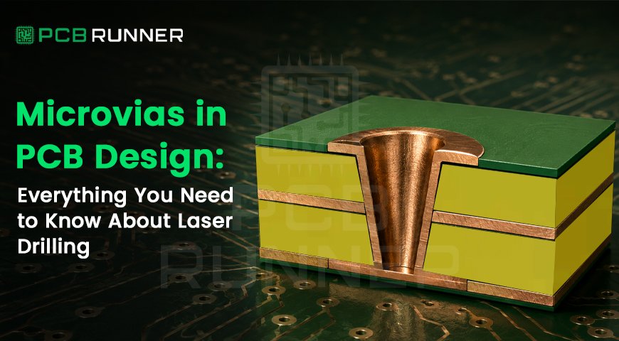
A microvia is a laser-drilled hole with a diameter of 6 mils or less, connecting one layer of copper foil to the immediately adjacent layer. Unlike a standard via, it doesn’t run through the entire board.
That distinction matters more than it sounds. Because a microvia only joins two neighboring layers, the layers above and below stay open for routing. On a dense board, that difference is what makes the layout work at all.
How Does Microvia Laser Drilling Actually Work?
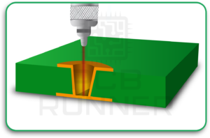
Laser drilling burns through one dielectric layer at a time, right after that layer gets added to the stack, rather than drilling through the whole finished board. The process happens in this order:
- A dielectric layer and copper foil get added to the substrate
- A laser drills straight down through that layer to the next foil beneath it
- The hole gets plated and filled with metal before the next layer goes on
- The next layer pair gets added, and the process repeats
This produces what’s called a buried microvia, since it’s fully enclosed once the surrounding layers are added. Filling the via with metal, rather than leaving it hollow, strengthens the connection and improves heat transfer through the board, which adds up to better long-term reliability.
What Is Sequential Build-Up and Why Does It Matter?
Sequential Build-Up, or SBU, adds layer pairs to the board one set at a time instead of pressing the whole stack at once. Each pair goes on symmetrically, one layer on each side of the core substrate, which balances stress across the board as it builds up.
For a substrate labeled N, the sequence looks like this:
- Layer 1 on each side: 1+N+1
- Layer 2 on each side: 2+N+2
- Layer 3 on each side: 3+N+3
Each layer gets its microvias drilled and filled before the next pair goes on. That’s the only way laser drilling can target a specific layer without drilling through layers that aren’t ready yet.
Where Do Microvias Get Used in Real Designs?
Microvias in PCB design show up wherever board space is limited and component density is high. A few common applications:
- Mobile phones and cameras: shrinking a device’s footprint depends on freeing up routing space that standard vias would consume
- 4G and 5G network hardware: dense circuitry in compact enclosures needs every available layer for routing, not via clearance
- Laptop and touch-screen devices: thinner boards with more components packed into less area
- Medical devices: compact, high-reliability boards where filled microvias also support better thermal performance
Via-in-pad designs are common across all four. Placing a via directly inside a component pad saves board space, but it risks a dry joint during reflow soldering if the via isn’t filled and plated flat first.
What Are the Real Benefits Over Mechanical Drilling?
Mechanical drilling works for standard through-hole vias, but it can’t reliably produce holes small enough for HDI-level density, and it drills through the entire board rather than targeting a single layer.
Microvia laser drilling offers a few specific advantages instead:
- Smaller hole diameter: down to 6 mils, well below what mechanical drilling can achieve reliably
- Layer-specific targeting: connects only adjacent layers, keeping the rest of the stack open for routing
- Stackable vias: filled and plated microvias can stack directly on top of one another, connecting three or more layers where needed
- Better thermal performance: metal-filled vias improve heat transfer compared to hollow or resin-filled equivalents
Stacking microvias in particular pushes circuit density further than a single layer-to-layer connection ever could, which is why HDI boards depend on it for the tightest layouts.
What Should You Check Before Specifying Microvias?
Confirm these details with your fabricator before finalizing a layout that depends on microvia laser drilling:
- Via fill method: confirm vias are filled and plated with metal, not left hollow, especially for via-in-pad designs
- Stacking requirements: if you need vias stacked across three or more layers, confirm the fabricator supports it reliably
- Layer sequencing: Sequential Build-Up needs to match your stackup, so confirm the process matches your layer count
- Clean room class: finer lines and annular rings require tighter process control, typically Class 100 clean room conditions
- Imaging method: contact imagery works for standard lines, but finer geometries usually need Laser Direct Imaging (LDI)
Get these confirmed against your actual HDI PCB stackup before committing to a final design, since via fill and layer sequencing both affect reliability down the line.
Microvias vs Standard Through-Hole Vias
| Factor | Microvias | Standard Through-Hole Vias |
| Diameter | 6 mils or less | Typically 8 mils or larger |
| Layer connection | Adjacent layers only | Full board, top to bottom |
| Drilling method | Laser | Mechanical |
| Routing space impact | Frees up space on non-connected layers | Consumes space across all layers |
| Stacking capability | Yes, when filled and plated | Not typically stacked |
| Best suited for | HDI, high-density boards | Standard multilayer boards |
Conclusion
Microvias in PCB design solve a routing problem that standard vias physically can’t. Laser drilling one layer at a time through Sequential Build-Up frees up space that a denser board simply doesn’t have to spare, and filled, plated vias keep that density reliable rather than fragile.
If you’re working through a high-density layout that’s running out of routing room, our team can review your stackup against our PCB Design and Laser Drilling capabilities. Submit your design files to sales@pcbrunner.com or engineering@pcbrunner.com, or call +44 203 2397011 to talk through your requirements directly.
FAQs
What’s the actual size limit for a microvia?
Ans: 6 mils in diameter or smaller. That’s the threshold that separates a microvia from a standard via drilled mechanically.
Can microvias be stacked on top of each other?
Ans: Yes, if they’re filled and plated with metal first. Stacked microvias can connect three or more layers, which increases design density beyond what a single via achieves.
Why does via-in-pad design need filled microvias specifically?
Ans: An unfilled via inside a pad can trap air or flux, leading to a dry joint during reflow soldering. Filling and plating the via keeps the pad surface flat and solderable.
Does laser drilling cost more than mechanical drilling?
Ans: Generally yes, since it requires more precise equipment and a layer-by-layer build process. The cost trade-off usually makes sense once board density exceeds what mechanical drilling and standard vias can support.
Do microvias work on rigid-flex or only rigid boards?
Ans: They’re used on both. The Sequential Build-Up process and laser drilling method apply the same way, though flex layers add extra considerations around material selection.



