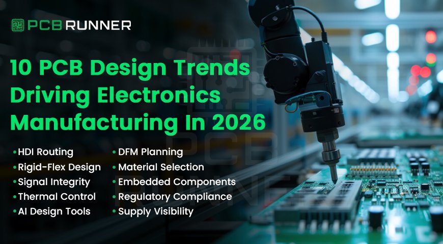
10 PCB Design Trends Driving Electronics Manufacturing In 2026
Objective This blog explains the biggest PCB Design trends shaping electronics manufacturing in 2026. It is written for those who […]
Objective This blog explains the biggest PCB Design trends shaping electronics manufacturing in 2026. It is written for those who […]
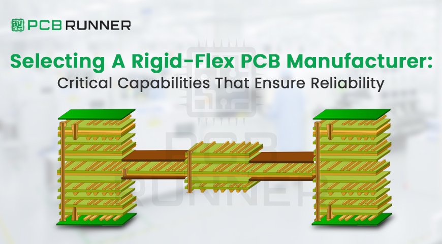
Objective This blog explains how to choose a Rigid Flex PCB Manufacturer with the right technical capabilities for reliable production.
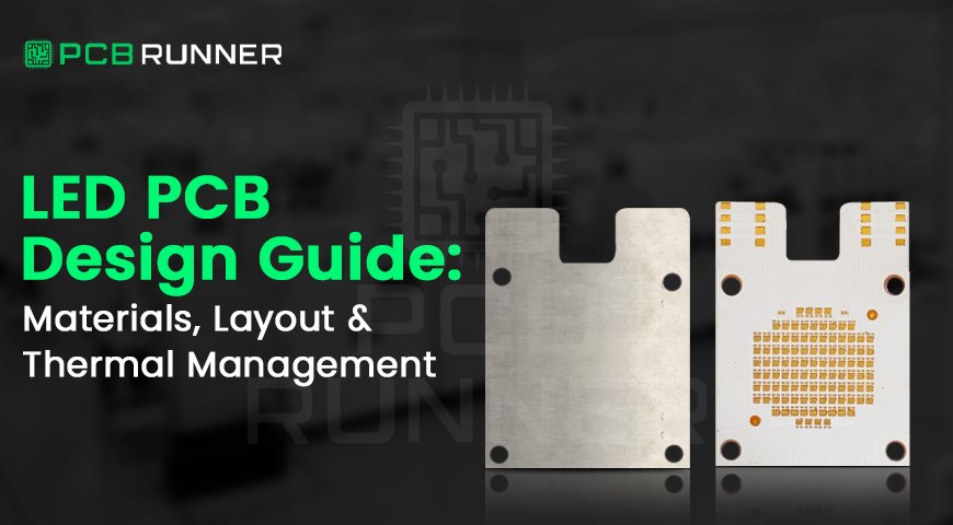
Objective This guide explains the practical side of LED PCB Design products. It covers board materials, layout choices, and heat

Objective This guide explains what really affects cost and lead time when choosing a PCBA Turnkey Manufacturing partner. It is
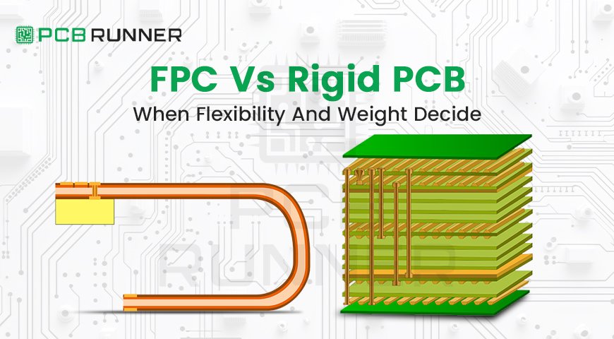
Objective This blog explains how to choose between a Rigid PCB and Flexible PCBs (FPCs) when space, movement, and weight
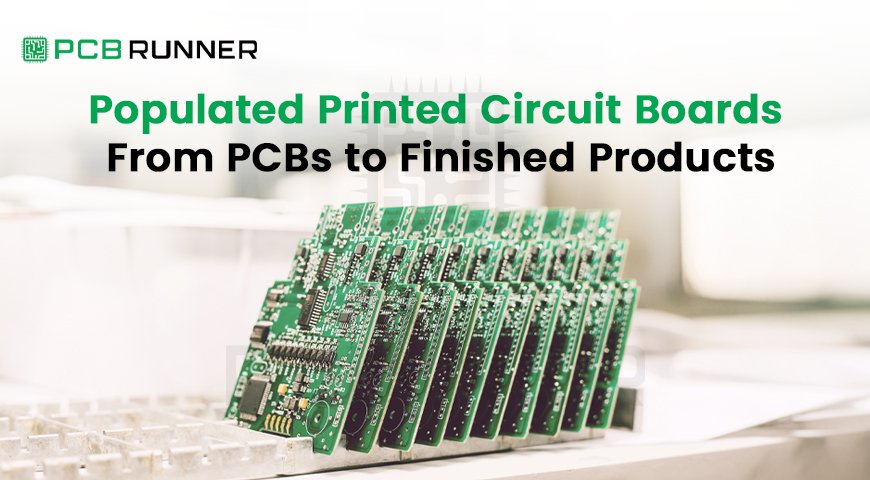
Objective Explain what a populated PCB is, how the PCB assembly process works from start to finish, and how populated
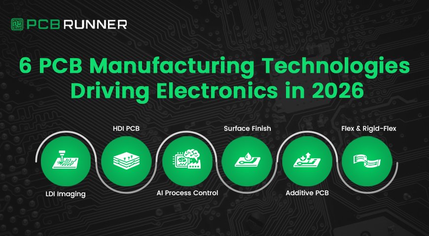
Electronics in 2026 are moving fast. Devices are smaller, chips run hotter, and designs pack more connections into less space.
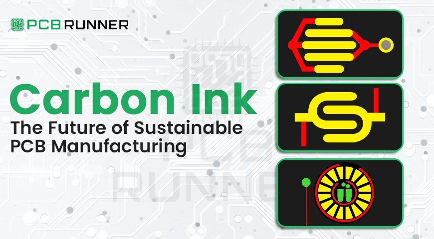
It is clear that the electronics sector is growing quickly, and sustainability is becoming an essential factor throughout every stage
When you send your design for PCB fabrication in Europe, there are many hidden steps that make sure your board
The process’s stability and dependability are key components of PCB manufacturing’s success. Strict tolerances must be upheld throughout the manufacturing

Fill out our comprehensive online PCB & Assembly specification form and receive instant pricing via email.

Have any advanced capability PCB design? Upload your files for our review and get a personalized quote from our Sales Engineer Executive via email.