


Objective
This blog post explains why heavy copper PCB plating becomes harder as copper weight climbs, what throwing power actually measures, and which plating methods keep via walls thick and consistent on 4oz-and-up boards. It’s written for design engineers and procurement teams specifying power electronics, motor drives, or high-current assemblies who need boards that survive thermal cycling instead of cracking at the via.
Key Takeaways
- Heavy copper PCB plating refers to depositing copper on boards with base layers of 3oz to 20oz per square foot, far beyond the 1oz to 2oz standard in most consumer electronics.
- Throwing power is the ratio between copper thickness at the center of a via and copper thickness at the board surface. Low throwing power means thin, unreliable via walls even when the surface looks fully plated.
- Standard DC plating struggles once via aspect ratio (hole depth divided by diameter) climbs past 6:1 to 8:1, which happens fast on thick copper boards with deep holes.
- Pulse-reverse plating, sectional plating, and controlled agitation are the three main tools fabricators use to push copper evenly into deep, narrow vias.
- IPC-6012 sets minimum via wall copper at 20 microns for Class 2 and 25 microns for Class 3. Heavy copper boards need process control well above these floors to hit reliable heavy copper via filling.
- Buyers should ask any manufacturer for cross-section reports and throwing power percentages before committing to a heavy copper run, not just a surface thickness spec.
Power electronics don’t fail quietly. A via with thin copper on one side and thick copper on the other runs hotter than it should, and after a few hundred thermal cycles, it cracks. That crack shows up as an intermittent fault on a board that passed every visual inspection. Nobody catches it until the product is in the field.
This is the problem throwing power was built to describe. Industry data shows that standard DC plating baths can leave via barrels with as little as 60% of the surface copper thickness once aspect ratios pass 6:1, a gap that gets worse as copper weight increases. Heavy copper PCB plating solves this, but only when the fabricator understands where and why standard processes break down on thick boards.
At PCB Runner, we build heavy copper boards for power distribution, industrial control, and high-current designs across the UK and Europe, and throwing power is one of the first things our engineering team checks before quoting a job. This guide walks through what causes uneven via plating on thick copper, and what separates a board that survives ten years of thermal cycling from one that doesn’t.
What Is Heavy Copper PCB Plating?
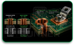
Heavy copper PCB plating puts down copper thickness of 3oz per square foot or more, well beyond the 1oz to 2oz used on standard boards.
Most commercial electronics use copper weights between half an ounce and 2oz per square foot. Once a design calls for sustained high current, that thin copper simply can’t carry the load without excessive resistive heating. Heavy copper starts at 3oz and commonly runs to 20oz; anything heavier falls into what the industry calls extreme copper.
The plating side of the process is where heavy copper gets complicated. Standard boards start with thin foil, etch away the unwanted copper, then plate up the remaining traces and via walls. On a heavy copper board, that same plating step has to deposit far more metal, evenly, inside holes that are often deep and narrow relative to their diameter.
Three things drive the demand for thick copper plating PCB construction:
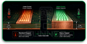
- High current carrying capacity. Doubling copper thickness roughly doubles the current a trace of the same width can carry without overheating.
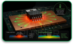
- Thermal mass. Thick copper planes act as heat spreaders, pulling heat away from hot components before it builds up.
- Mechanical durability. Heavier copper at plated through-holes and connector pads holds up better under vibration and repeated thermal expansion.
What Is Throwing Power and Why Does It Matter?
Throwing power is the ratio of copper thickness inside a via to copper thickness on the board surface, expressed as a percentage.
If a plating process deposits 2 mils of copper on the surface but only 1.2 mils at the center of a via wall, that process has 60% throwing power for that hole geometry. The industry treats anything below roughly 70% as a reliability risk for critical applications, and IPC-6012 Class 3 work typically demands tighter control than that.
Throwing power drops for a simple reason: current density inside a deep, narrow hole is much lower than current density at the open board surface. Ions have a harder path to travel to reach the center of the hole. The plating bath deposits copper fastest where current density is highest, which is the surface and the top edges of the via, not the middle of the barrel.
This matters because a via isn’t just an electrical connection. On a heavy copper board carrying real current, the via barrel is also a thermal and mechanical path. A thin spot in the middle of that barrel is a failure point waiting for a thermal cycle to find it.
Why Do Thick Copper Boards Struggle with Even Plating?
Three factors compound on heavy copper boards and make throwing power harder to hold than it is on standard-weight designs.
- Aspect ratio climbs fast.
Aspect ratio is hole depth divided by hole diameter. A 3.2mm thick heavy copper board with a 0.4mm drilled hole already sits near 8:1, a point where standard DC plating starts losing grip on the via center. Push the board thicker or the hole smaller, and the math only gets worse. - Current density becomes harder to balance.
Wide copper planes and isolated fine traces pull current very differently during plating. On a heavy copper layout with both large pours and narrow high current PCB manufacturing traces, the plater has to balance deposition across features that behave nothing alike. - Gas evolution and trapped air inside deep holes.
Deep, high-aspect-ratio holes trap air and hydrogen gas generated during electrolysis. That trapped gas blocks the plating solution from reaching the via center, creating voids that show up on cross-section but not on a surface inspection.
How Do Manufacturers Improve Copper Throwing Power?
Fabricators use a combination of process changes, not a single fix, to bring throwing power up to acceptable levels on 4oz copper PCB work and heavier.
- Pulse-reverse plating. Instead of running current in one direction continuously, pulse-reverse plating alternates forward and reverse pulses. The reverse pulse strips back over-plated high-current-density spots, forcing more even distribution into the via center. Properly tuned pulse-reverse processes can reach fill ratios well above what conventional DC plating achieves on the same aspect ratio.
- Differential and step etching. Rather than etching thick copper away in one pass, fabricators etch in controlled stages. This keeps trace sidewalls straighter and reduces the undercutting that plagued early heavy copper boards plated with older, single-pass methods.
- Reduced initial current density. Running lower current for the first 15 to 20 minutes of a plating cycle gives gas a chance to clear before copper coverage locks in, cutting down on voids at the via wall.
- Improved bath agitation. Eductors, spray systems, and optimized flow paths keep fresh plating solution moving through the hole instead of stagnating at the center, which is where throwing power problems concentrate.
- Leveling and brightening additives. Modern acid copper baths use additive packages designed specifically to slow deposition at high-current areas and encourage it at low-current areas like the via center.
What Does Good Heavy Copper Via Filling Look Like?
Heavy copper via filling is judged by cross-section, not by eye. A fabricator cuts a sample coupon through the via, polishes it, and measures copper thickness at the top, middle, and bottom of the barrel under a microscope.
What good looks like, in practice:
- Minimum via wall thickness at 70% or more of nominal surface thickness for standard aspect ratios (typically up to 6:1 or 8:1 depending on class)
- No visible voids or trapped-air pockets at the via center
- Consistent copper thickness from top to bottom, not just a thick cap with a thin core
- Straight via sidewalls without excessive dishing or thinning at the midpoint
For boards using filled and capped vias under BGAs or high-power components, the standard tightens further, since any void becomes a thermal bottleneck directly under the heat source.
Design choices also affect how achievable good throwing power is before the board ever reaches the plating line. Keeping via aspect ratio at 6:1 or below, and closer to 4:1 for critical thermal vias, gives the plating process a real chance of hitting spec instead of fighting geometry it can’t overcome.
DC Plating vs. Pulse-Reverse Plating: A Comparison
| Factor | Standard DC Plating | Pulse-Reverse Plating |
| Typical via fill at 8:1 aspect ratio | ~60% of surface thickness | Up to 90%+ with optimized parameters |
| Best suited for | Lower aspect ratio, thinner copper boards | Heavy copper, high aspect ratio vias |
| Gas/void control | Weaker, more prone to trapped air | Stronger, reverse pulse helps dislodge gas |
| Process complexity | Simpler, lower equipment cost | Requires tuned rectifiers and process control |
| Reliability at Class 3 spec | Adequate for moderate thickness | Preferred for critical, high-current designs |
What Should You Check Before Ordering Heavy Copper Boards?
A quote that only lists copper weight tells you almost nothing about whether the fabricator can actually hit reliable throwing power on your design. Before placing an order for power electronics PCB fabrication, ask for:
- Cross-section reports from a prior job at a similar copper weight and aspect ratio, not just a spec sheet.
- Stated throwing power percentage for the aspect ratios your design uses.
- IPC class certification (Class 2 or Class 3) and confirmation of which class applies to your via plating requirement.
- DFM feedback specific to heavy copper, covering trace spacing, annular ring, and via aspect ratio before the board goes to fabrication.
- Confirmation of plating method used for high-aspect-ratio holes, since not every shop runs pulse-reverse capability.
You can read more on copper thickness selection in our guide to PCB standard and heavy copper thickness, and on protecting these boards from interference in our piece on shielding techniques in heavy copper PCBs.
Cost rises with copper weight, mostly because of longer plating cycles, slower etch stages, and the extra inspection heavy copper work demands. A 6oz board with tight aspect ratio control isn’t priced the same as a 1oz board with the same layer count, and any quote that doesn’t reflect that gap is worth a second look.
FAQs
Is heavy copper PCB plating more expensive than standard plating?
Yes, generally. Longer plating cycles, step etching, and added cross-section inspection all add cost. The increase is usually justified once you factor in the current capacity and thermal life you gain.
What copper weight counts as heavy copper?
Most of the industry treats 3oz per square foot and above as heavy copper, with true “extreme copper” starting past 20oz.
Can throwing power problems be fixed after the board is manufactured?
No. Throwing power is a plating-stage issue. Once the board is built, thin via walls can only be caught through inspection, not corrected. That’s why cross-section verification before full production matters.
Does via aspect ratio matter more than copper weight for throwing power?
Both matter, but aspect ratio drives the physics more directly. A thick board with wide, shallow vias plates far more evenly than a thin board with deep, narrow ones.
How do I know if my design needs pulse-reverse plating?
If your via aspect ratio is above 6:1, or your board uses 4oz copper or heavier with plated through-holes carrying real current, pulse-reverse plating is worth specifying rather than leaving it to the fabricator’s default process.
Conclusion
Throwing power isn’t a footnote in heavy copper fabrication, it’s the difference between a board that lasts and one that fails quietly in the field. Getting it right takes the right plating chemistry, the right via geometry from the design stage, and a fabricator willing to show you cross-section data instead of a surface spec sheet.
If you’re specifying a heavy copper PCB plating project, our engineering team reviews your Gerber files and stack-up for aspect ratio and throwing power risk before quoting, at no charge. Reach out to engineering@pcbrunner.com or sales@pcbrunner.com, or call +44 203 2397011, and read more on our process in heavy copper PCB manufacturing and benefits.



