


Expert Buried Via PCB Manufacturing Solutions – Enhance Your PCB Design
Buried Via PCB In a multi-layer PCB, buried vias are plated connections between the inner layers that are not visible

Buried Via PCB In a multi-layer PCB, buried vias are plated connections between the inner layers that are not visible
High Production Volume, High Quantities of PCBs After the verification of the prototype, do you intend to produce PCBs in
Stacked Vias: What Does It Mean? Stacked vias are created by stacking numerous vias on top of one another. To
Consider using a loose-leaf approach to the stack-up in the bend regions of flex when there are four or more
The metallization of a circuit board’s edges is known as side plating, sometimes known as edge plating or Castellation, in
Harnessing the Power of Effective PCB Routing: Strategies, Best Practices, and Future Trends In the realm of printed circuit boards,
PCB Solder Mask Guide: Types, Colors & Design Tips Introduction: Printed circuit boards (PCBs) are coated with a polymer layer
Exploring PCB Via Types: Choosing the Right Vias for Your Design Needs Introduction Vias are holes that allow conductivity to

Mastering PCB Design: From Schematic to BOM and Production – A Comprehensive Guide by PCB Runner A consistent visual depiction
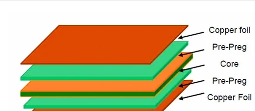
In essence, PCB cores are one or more prepreg laminates that have been heated, pressed, hardened, and cured. Copper foil
Fill out our comprehensive online PCB & Assembly specification form and receive instant pricing via email.
 +44 203 2397011
 sales@pcbrunner.com
Have any advanced capability PCB design? Upload your files for our review and get a personalized quote from our Sales Engineer Executive via email.
+44 203 2397011sales@pcbrunner.com