



Objective
This guide gives design engineers and procurement teams a practical way to answer one recurring question: how many layers does this board actually need? It covers the real drivers behind multilayer PCB layer count decisions, how stack-up planning changes the answer, and where over-speccing layers quietly inflates cost without adding value.
Key Takeaways
- Multilayer PCB layer count should follow routing density, signal integrity needs, and power distribution, not a round number picked out of habit.
- Pin density is a strong early indicator. Dense, fine-pitch parts with tight spacing push designs toward 8 layers or more; simple analog boards often route fine on 2.
- Every high-speed signal layer wants an adjacent reference plane. That single rule is what pushes most “just add two more layers” decisions.
- Layer count cost trade-off isn’t linear. Going from 2 to 4 layers is a modest jump; going past 12 layers brings sequential lamination, tighter registration tolerances, and real cost increases.
- Good multilayer PCB stack-up planning happens before layout starts, not after routing gets stuck.
- Talking to your fabricator early, before finalizing layer count, catches manufacturability issues that are expensive to fix once the design is locked.
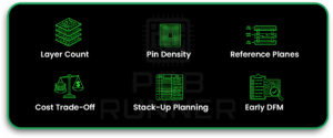
One of the most common mistakes in multilayer PCB design is assuming that adding more layers automatically improves the board. In reality, every additional layer increases fabrication complexity, affects stack-up design, and adds manufacturing cost. The goal isn’t to maximise layer count, it’s to use the fewest layers that satisfy routing density, signal integrity, power distribution, and reliability requirements.
Industry guidance is consistent on the core driver: pin density is one of the strongest predictors of layer count, with a pin density around 1.0 often routing on 2 signal layers, while density below 0.2 can push a design past 10 layers. Choosing PCB layer count correctly means matching the number to what the design actually needs, not defaulting to whatever the last project used.
At PCB Runner, our engineering team runs layer count and stack-up review as a standard part of DFM feedback on every multilayer quote, across rigid, flex, and rigid-flex builds for customers throughout the UK and Europe. This guide breaks down how that decision actually gets made.
What Determines Multilayer PCB Layer Count?
Layer count comes down to three things: how much needs to be routed, how clean the signals need to stay, and how much current and heat the board has to manage.
These three forces pull in different directions, and the final layer count is wherever they land.
- Routing density. More components, finer pin pitch, and tighter board outlines all mean less room per layer. When traces can’t fit without violating spacing rules, the answer is usually another layer, not a smaller trace width.
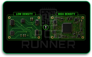
- Signal integrity requirements. High-speed interfaces like DDR memory, PCIe, USB 3.0, or HDMI need controlled impedance. That means every signal layer needs an adjacent, unbroken reference plane, which by itself can add two or more layers to a board that would otherwise route fine.
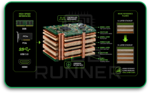
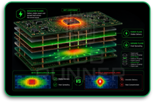
- Power and thermal demands. Boards carrying meaningful current benefit from dedicated power and ground planes, both for stable delivery and for spreading heat across the board rather than concentrating it at hot components.
How Many Layers Does a Simple Design Actually Need?
Not every board needs to be complicated, and forcing extra layers onto a simple design just adds cost without a payoff.
- 2 layers: Fine for basic analog circuits, simple sensor boards, and low-pin-count microcontroller designs with modest component counts.
- 4 layers: The practical default for moderate complexity. A 4-layer stack-up typically gives you a signal, ground, power, and signal layer, which handles most general-purpose digital designs cleanly.
- 6 layers: Where designs start needing dedicated reference planes for more than one high-speed interface, or where component density on a 4-layer board is forcing trace widths tighter than you’d like.
If your board fits comfortably in one of these tiers with routing to spare, adding layers “for safety margin” is usually money spent for nothing.
When Do High-Speed and Dense Designs Require More Layers?
Once a design includes fine-pitch BGAs, multiple high-speed interfaces, or tight EMI requirements, 8 layers and up becomes the realistic starting point.
A few patterns show up consistently in designs that outgrow lower layer counts:
- Fine-pitch BGAs and dense connectors. Breaking out a 0.4mm pitch BGA without blind or buried vias eats routing channels fast. Extra layers give escape routing somewhere to go.
- Multiple simultaneous high-speed buses. A board running DDR memory alongside PCIe and a high-speed serial link needs separate, well-referenced layers for each, since they can’t safely share a plane without crosstalk risk.
- Mixed analog and digital domains. Keeping sensitive analog sections isolated from noisy digital switching often means dedicating layers specifically to separation, not just routing.
- EMI-sensitive or regulated applications. Aerospace, medical, and automotive designs commonly specify extra ground layers purely for shielding and compliance, independent of routing need.
High current PCB manufacturing situations follow a related but different logic. Here the extra layers aren’t about routing channels, they’re about copper cross-section for current capacity and heat spreading, which is a separate conversation from signal layer count.
How Should You Plan a Multilayer PCB Stack-Up?
Multilayer PCB stack-up planning is the step between “we need roughly this many layers” and a finished, manufacturable layer order. Skipping it is one of the most common reasons boards go back for redesign mid-project.
Good stack-up planning covers:
- Layer function assignment. Decide early which layers are signal, which are power, and which are ground, rather than discovering the gaps once routing starts.
- Reference plane placement. Every critical signal layer should sit next to an unbroken ground or power plane. Splitting planes to solve a routing problem usually creates a signal integrity problem instead.
- Symmetry. A symmetric stack-up, matched copper weight and dielectric thickness on either side of the board’s center, reduces warpage during lamination and keeps the board flatter through assembly.
- Impedance targets. If any signal needs controlled impedance, that requirement has to be built into the stack-up from the start; it can’t be bolted on after layout is finished.
- Fiber weave orientation. Rotating glass weave direction between adjacent dielectric layers helps with dimensional stability, particularly relevant once layer count and board thickness both climb.
You can see how this plays out on advanced boards in our guide to choosing the right stackup for your HDI PCB design, where via strategy and layer order interact even more tightly than on a standard multilayer build.
What Is the Real Layer Count Cost Trade-Off?
Layer count cost doesn’t scale in a straight line, and knowing where the curve bends helps set realistic budget expectations.
| Layer Range | Typical Cost Behavior | What Drives It |
| 2 to 4 layers | Lowest relative cost, minimal tooling complexity | Single lamination cycle, standard drilling |
| 6 to 8 layers | Moderate step up | Additional lamination, tighter registration control |
| 10 to 14 layers | Noticeable jump | Sequential lamination cycles, longer cycle time |
| 16+ layers | Highest relative cost per layer added | Multiple lamination passes, blind/buried via drilling, tighter tolerances |
The jump from 4 to 6 layers is usually modest. The jump from 10 to 16 is not, because sequential lamination, more precise registration, and often blind or buried vias all enter the picture together. This is exactly where an unnecessary layer or two, added out of caution rather than need, does the most damage to a quote.
Layer Count by Application: A Quick Reference
| Application Type | Typical Layer Count | Primary Driver |
| Simple sensor or analog board | 2 layers | Low component count, low routing density |
| General digital / consumer electronics | 4 layers | Balanced routing with dedicated power/ground |
| Mixed-signal or single high-speed interface | 6 layers | Signal integrity, moderate density |
| Multi-interface high-speed digital | 8 to 10 layers | Multiple reference planes, dense BGAs |
| Networking, RF, or advanced computing | 10+ layers | High routing density, strict impedance control |
| Aerospace, medical, military | Varies, often higher | EMI shielding, redundancy, compliance |
What Should You Ask Your Fabricator Before Finalizing?
A layer count that looks fine in your CAD tool can still run into manufacturability issues that only show up once a fabricator reviews the stack-up. Before locking the design, ask about:
- Minimum trace width and spacing the fabricator can hold reliably at your target layer count and copper weight.
- Blind and buried via capability, if your routing density needs them, since not every shop supports both on the same board.
- Registration tolerance for your layer count, particularly past 10 layers where sequential lamination adds cumulative shift risk.
- Standard versus custom stack-up pricing. Some layer counts and dielectric combinations sit on a fabricator’s standard menu; others require custom tooling that adds cost and lead time.
- DFM feedback on the specific design, not just a generic layer count recommendation. The same layer count can be easy or difficult to build depending on component placement and via strategy.
Our team reviews Gerber files and layer stack-ups as a standard part of every quote, and flags routing or registration risk before the board goes to fabrication rather than after.
FAQs
Is a higher layer count always more reliable?
Not automatically. More layers give more routing room and better signal isolation, but a poorly planned high layer count can introduce its own reliability risks through registration drift and lamination stress. Reliability comes from a well-planned stack-up, not layer count alone.
Can I reduce layer count after my design is already routed?
Sometimes, but it usually means re-routing sections rather than a simple layer deletion, since removing a reference plane affects impedance and crosstalk on the signals around it.
Do all 4-layer PCBs use the same stack-up?
No. A standard 4-layer stack-up (signal, ground, power, signal) is common, but the exact copper weights, dielectric thickness, and plane split depend on your current and impedance requirements.
How do I know if my design needs blind or buried vias?
If routing density on your target layer count is forcing trace widths or spacing tighter than your fabricator’s standard capability, blind and buried vias are usually the next step before adding a full layer pair.
Does layer count affect PCB lead time?
Yes. Boards above roughly 10 to 12 layers typically need sequential lamination cycles, which adds production time compared to a single-press 4 or 6-layer build.
Conclusion
The right multilayer PCB layer count isn’t the highest number you can justify, it’s the smallest number that routes cleanly, holds signal integrity, and meets your thermal and power needs. Getting there takes an honest look at routing density and signal requirements before layout starts, not a guess carried over from your last project.
If you’re sizing a new multilayer design, send us your schematic and component list and our engineering team will help estimate layer count and review stack-up options at no charge. Reach out to engineering@pcbrunner.com or sales@pcbrunner.com, or call +44 203 2397011, and read more in our multilayer PCB guide and our overview of what a multilayer PCB is.



