


A multilayer PCB is a set of more than two copper foils placed together in a single PCB unit, with each foil insulated from the others.
Its structure consists of double-sided inner layers and single-sided outer layers at the top and bottom.
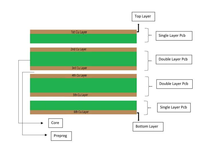
A Multilayer PCB Core is coated with copper foil on both sides. Heat is used to cure and solidify it, making it more durable than prepreg. Prepreg, which is made of woven glass cloth and epoxy resin, is used as an isolating material between copper layers and cores.
Through-hole components have connections to all layers with their own through-hole plated pads, whereas surface-mounted components are connected through vias. In multilayer PCBs, there are three different types of vias that are utilized: Buried Vias, Blind Vias, and Through Hole Vias.
All these three types of connectivity services can provided by leading manufacturers like PCB Runner, which are established in the UK and Europe.
Significance of multilayer PCB in modern technology
The capacity of multilayer PCBs to fit more components into a smaller area is one of their primary benefits. Designers can reduce the total size and weight of the PCB by more effectively distributing the circuitry by utilizing multiple layers. Particularly useful for small electrical devices like wearables, tablets, and smartphones.
In addition, multilayer PCBs provide better signal integrity than single-layer and double-layer models. In order to provide clear and reliable signal transmission, extra layers, as well as dedicated power and ground planes, aid in lowering noise and interference. For sensitive analog applications and high-speed digital circuits, multilayer PCBs are important. Depending on the design specifications and circuit complexity, a multilayer printed circuit board (PCB) may have one or more layers.
In complex analog designs, controlled impedance tracks are under special consideration to avoid cross-talk in the design. We at PCB Runner verified the functionality of providing the required technical data and carried out different tests to make the design successfull and fully functional.
Our Multilayer PCB Manufacturing Capabilities
|
Parameters |
Specifications |
|
Layers |
1-50 layer |
|
Board Material |
Rigid: FR4: KB6164, KB6167, S1000-2M, S1000H, TG150: KB6165 Rogers: R4350B, R4003C Metal Core: T111 AL Halogen: S1150G TG135:ShengyiS1141/ KB6160 (CTI175-249)Polymide: Thinflex PI, Panasonic PI
|
|
The impedance value and tolerance |
minimum 40+/-5% ohm & max 120ohm +/-10% |
|
Inner line width/ Line spacing (original) |
For Rigid: 1oz = minimum 3 mil& max no limited 2oz = minimum 6 mil 3oz = minimum 8.5 mil 4oz = minimum 11 mil 5oz = minimum 14 mil 6oz = minimum 18 mil
For Flex: 1oz = minimum 2.5mil & max not limited. 2oz = minimum 6 mil 3oz = minimum 8 mil |
|
The group of impedance |
min & max, no group QTY limited, we can calculate the impedance per your spec |
|
Vias |
Blind, Buried, Plugged, Via-in-Pad, Micro via |
|
BGA PITCH |
minimum 0.10mm- max 0.12(mm) |
|
Blind VIA / BURRIED VIA |
minimum – max (mm) Stacked 0.10mm Staggered 0.10mm |
|
Laser Drill Size |
Minimum (mm) 0.10 Max (mm) 0.12 |
|
Aspect Ratio |
Laser Drill (minimum 1:1.3& standard 1:1) Mechanical Drill (minimum 1:12& standard 1:8) |
|
Tests |
Flying Probe test OR E-Test Functional testing for the specific design Impedance Test Solderability Test Stress test for Pcbs Hole wall copper plating test to ensure required thickness. |
Design Considerations for multilayer PCB
The following are the factors that are under consideration while designing multilayer PCBs.
Choosing the Right Type:
There are four types of multilayer PCB that can be considered before designing:
- Rigid Multilayer PCBs
- Flex Multilayer Circuits
- Rigid-Flex Multilayer PCB
- Metal Core Multilayer Boards
Designing Layer Stackup:
Layer stackup is the primary distinction between multilayer and single/double layer Pcb. Performance, density, circuitry, and cost are factors that are associated with the layer stack. After choosing the material based on the functionality of your circuit, it is crucial to organize the layers based on the results of your impedance calculation and the functionality of your circuitry. The next steps are taken after determining layer management and count. Careful calculations must be made in accordance with the design, as the addition and subtraction of a single layer might cause pain throughout the entire procedure after the layer stack is complete.
Component Placement:
Placing printed circuit board components is the second critical step after choosing a layer stack. Place analog-sensitive components away from digital circuits to prevent signal interference and maintain reliable circuit performance. Similarly, position RF components carefully and use adequate ground shielding to minimise EMI/EMC issues. In addition, place coupling and decoupling capacitors as close as possible to the corresponding IC pins to ensure stable power delivery and reliable operation. After completing proper placement, it is easy to handle the routing of tracks.
Power Distribution and thermal management:
In Pcb design, the distribution of power is a key aspect of electronic design that needs to be planned and thought out carefully. While a poorly constructed network can result in problems like voltage drop, overheating, and component failure, a well-planned power distribution network can guarantee the dependability and performance of the electronic device. Similarly, thermal management of power-generating components is very necessary. To control the board’s temperature, a variety of heat dissipation strategies can be used, such as the placement of heat sinks, thermal pads, and thermal vias.
Signal Integrity:
When choosing trace lengths and layer thicknesses for high-speed signals, take care to provide controlled impedance.
>To preserve signal integrity, use appropriate routing approaches, such as avoiding sharp and rough bends and making sure that trace lengths are constant. To prevent electromagnetic interference (EMI) and electromagnetic compatibility (EMC) problems, use ground planes and shielding techniques.
Keep noisy or high-frequency signals away from sensitive traces to minimize cross-talk.
Compliance and Standards:
Make that the design complies with industry standards and guidelines relevant to the particular application, such as RoHS (Restriction of Hazardous Substances) compliance, IPC Class 2, and IPC Class 3.
Manufacturability:
Designers should evaluate their PCB manufacturer’s capabilities before starting the design. They should also follow the manufacturer’s minimum and maximum manufacturing specifications to ensure the board is easy to fabricate, reduces production issues, and meets quality standards.
Circuit board manufacturers require accuracy while handling complicated designs. When designing a complicated design, cooperation, and communication with the manufacturer are essential because it helps save money, effort, and time for all involved.
Conclusion
Before selecting a PCB manufacturer for your multilayer PCBs, check whether the company employs a skilled engineering team with expertise in the latest PCB technologies. This ensures you receive an optimised design from the outset, thereby increasing the likelihood of completing your project on time. The manufacturer should provide guidance on selecting the most suitable materials for your application. Ultimately, this collaboration helps improve performance, manufacturability, and long-term reliability.
In UK and Europe, there are few manufacturers like PCB Runner who can do everything under one roof. To get white gloves service, feel free to contact us or get a free quote now!
FAQs
1. What is a multilayer PCB?
A multilayer PCB is a printed circuit board with three or more conductive copper layers separated by insulating material. It enables compact designs, higher component density, and improved signal integrity for complex electronic devices.
2. What are the advantages of multilayer PCBs?
Multilayer PCBs provide higher circuit density, better signal integrity, improved EMI performance, reduced board size, and enhanced reliability for high-speed and high-power applications.
3. How many layers can a multilayer PCB have?
Most multilayer PCBs use 4 to 12 layers. However, advanced applications such as servers, telecommunications, aerospace, and AI hardware often require 16, 24, or even 50 layers because they demand higher routing density, better signal integrity, and greater performance.
4. What materials are used in multilayer PCB manufacturing?
Common materials include FR-4, Rogers laminates, polyimide, metal-core substrates, and high-Tg materials. The material choice depends on thermal performance, operating frequency, and application requirements.
5. What are the different types of vias used in multilayer PCBs?
Multilayer PCBs commonly use through-hole vias, blind vias, buried vias, microvias, and via-in-pad technology to create electrical connections between different copper layers.
6. Why is layer stackup important in multilayer PCB design?
A properly designed layer stackup improves signal integrity, controls impedance, reduces EMI, enhances power distribution, and simplifies manufacturing, making it one of the most critical aspects of multilayer PCB design.



