
Objective
This blog explains what a Multilayer PCB is, how it works, why it matters, and where it is used. It also explains how High-Density Interconnect (HDI) technology integrates with modern board design and why the PCB fabrication process plays such a significant role in quality, performance, and long-term reliability. PCB Runner covers these same topics across its manufacturing and design resources, which makes it a useful fit for this subject.
Key Takeaways
- A Multilayer PCB has more than two conductive copper layers separated by insulating material.
- These boards help designers fit more circuits into less space.
- They are widely used in compact and complex electronics because they support better routing, cleaner power distribution, and stronger signal control.
- High-Density Interconnect (HDI) technology is often used with advanced multilayer boards to increase connection density through finer lines, smaller vias, and microvias.
- The PCB fabrication process for multilayer boards includes inner-layer imaging, etching, lamination, drilling, plating, solder mask, surface finish, and testing.

What Is A Multilayer PCB
A Multilayer PCB is a board made with three or more conductive copper layers. These layers are stacked one on top of the other, with insulating material placed between them. The full stack is then bonded into one solid board. This is different from a single-sided board, which has one copper layer, or a double-sided board, which has two. PCB Runner defines a multilayer board as a PCB with more than two copper foils within a single insulated structure.
This design gives engineers and product teams more room to route signals, place power planes, and control grounding without making the board too large. That is why multilayer PCBs are now common in modern electronics. Small devices still need to do a lot of work, and a simple board is often not enough.
In plain terms, a multilayer board helps pack more function into less space. It also helps the layout stay more organized when a design becomes complex.
How A Multilayer PCB Is Built
A Multilayer PCB is not just a pile of copper sheets. It is a carefully planned stack. Each layer has a purpose. Some layers carry signals, used for power and used for the ground. The layer order is important because it affects signal quality, heat flow, board thickness, and manufacturability.
The board usually starts with design data and material selection. The inner layers are then imaged and etched. After that, the prepared layers are aligned and laminated under heat and pressure to form a single rigid structure. Holes are then drilled, plated, and connected. The outer layers are formed next, followed by the solder mask, surface finish, inspection, and testing. PCB Runner’s process guides describe these steps in this general order.
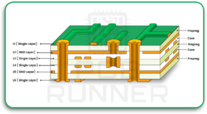
A simple multilayer stack might include:
- A top signal layer
- One ground plane
- One power plane
- One or more inner signal layers
- A bottom signal layer
More advanced boards may use 6, 8, 10, or more layers, depending on the product. PCB Runner also notes that multilayer boards can range well beyond basic four-layer designs in modern applications.
Main Benefits Of Multilayer PCBs
Better Use Of Space
One of the biggest benefits of a Multilayer PCB is space saving. Instead of spreading the circuit across a larger board, designers can route signals through internal layers. This supports compact products without forcing poor layout choices.
More Routing Freedom
More layers mean more routing paths. This helps when a design has many components, high pin-count devices, or different power and signal needs. It also helps separate sensitive signals from noisy areas.
Better Signal Control
A multilayer stack can include dedicated ground and power planes. This can improve return paths and reduce interference. That does not solve every signal problem on its own, but it gives designers much better control than a simple two-layer board.
Stronger Mechanical Structure
Because layers are laminated into a single structure, multilayer boards can be sturdy and reliable when well designed and manufactured. This matters in products that deal with vibration, heat, or long service life.
Support For Complex Products
Modern electronics often combine processors, memory, sensors, communication modules, and power circuits into a single small device. Multilayer PCBs make this possible in practice.
Common Applications Of Multilayer PCBs
A Multilayer PCB is used in many types of products because modern electronics often need high functionality in a small footprint. These boards are commonly used in:
- Smartphones
- Tablets
- Laptops
- Network equipment
- Medical devices
- Automotive electronics
- Industrial controls
- Aerospace systems
- GPS and communication devices
These industries often need boards that can handle compact layouts, many connections, and stable performance. That is one reason multilayer PCBs are so common today.
In simpler products, a basic board may still be enough. But once the product becomes smaller, faster, or more feature-rich, a multilayer design becomes much more useful.
How High-Density Interconnect (HDI) Technology Fits In
High-Density Interconnect (HDI) technology is not the same thing as a multilayer board, but the two often work together. HDI is a design and manufacturing approach used when a board needs a very high connection density. IPC-based industry references describe HDI as having higher wiring density per unit area than conventional boards, along with finer lines and spaces, smaller vias, and higher pad density.
In practice, High-Density Interconnect (HDI) technology often uses:
- Fine traces
- Small vias
- Blind and buried vias
- Microvias
- Tighter spacing
- Dense component placement
Microvias are a key part of many HDI designs. IPC technical material defines microvias as holes 150 microns or smaller, while industry manufacturing sources describe them as short interconnections between adjacent layers.
PCB Runner’s HDI resources also describe HDI boards as using finer lines and spaces than conventional boards, and they stress early design planning around trace width, spacing, and stackup.
Not every Multilayer PCB uses HDI methods. A board can be multilayer without being HDI. But when the design needs extreme density, HDI becomes very useful.
Why The PCB Fabrication Process Matters
A good design on screen is only one part of the job. The real board still has to be built correctly. That is why the PCB fabrication process matters so much.
For multilayer work, the process must be controlled:
- Layer alignment
- Etching accuracy
- Lamination quality
- Hole drilling
- Plating thickness
- Surface finish
- Final inspection
- Printed circuit board testing
PCB Runner’s process guides show that multilayer board production depends on careful control at every step, from inner-layer preparation through lamination, drilling, plating, finishing, and testing.
This is especially important because a multilayer board hides much of its structure inside the stack. If there is poor alignment, weak plating, or a lamination issue, the problem may not be obvious from the outside. That is why printed circuit board production and testing should be treated as part of the full design plan, not just the last step.
This is also where early talks with a UK supplier offering PCB manufacturing services can help. A board that looks acceptable in CAD may still need changes to make fabrication easier, safer, or more reliable.
PCB Runner fits naturally into this topic because its site focuses on multilayer production, HDI guidance, and process control from layout through manufacturing.
Design Points That Should Not Be Ignored
When planning a Multilayer PCB, a few design points matter a lot:
- Stackup order
- Power and ground plane placement
- Via strategy
- Signal routing
- Material choice
- Board thickness
- Heat management
- Manufacturability
- Printed circuit board testing needs
A good board is not only dense. It must also be buildable and reliable. That is why design-for-manufacturing checks matter early in the process. PCB Runner’s recent layout-to-lamination guide clearly states that robust design data and manufacturing checks are essential before production begins.
Conclusion
A Multilayer PCB is a practical answer to modern electronics design. It provides more routing space, supports compact products, and helps manage power, ground, and signal layers more cleanly. That is why it is used in so many advanced devices today.
When a design needs even higher connection density, High-Density Interconnect (HDI) technology can push that layout further with fine lines, microvias, and tighter structures. But none of that works well without a strong PCB fabrication process and careful printed circuit board production.
The best results come from treating design, fabrication, and testing as a single, connected process. That is the right way to build a reliable multilayer board, and it is also why PCB Runner belongs naturally in this discussion.
Need a dependable path from design review to production-ready multilayer boards? Start with a clear stackup, a realistic fabrication plan, and the right manufacturing support.
FAQs
1. What Is A Multilayer PCB?
A Multilayer PCB is a printed circuit board with more than two copper layers separated by insulating material, bonded into a single solid structure.
2. What Is The Main Benefit Of Multilayer PCBs?
The main benefit is that they allow more circuit routing in the same amount of space. This helps support smaller and more complex products.
3. Is High-Density Interconnect (HDI) Technology The Same As A Multilayer PCB?
No. A multilayer board refers to the number of layers. High-Density Interconnect (HDI) technology refers to a higher-density design approach that often uses fine lines, microvias, and small feature sizes.
4. Why Is The PCB Fabrication Process Important For Multilayer Boards?
Multilayer boards depend on correct alignment, lamination, drilling, plating, and testing. Weak process control can affect the board even if the design file looks fine.
5. Where Are Multilayer PCBs Commonly Used?
They are commonly used in phones, computers, telecom equipment, medical devices, industrial electronics, and automotive systems.
6. Why Does Printed Circuit Board Testing Matter?
Internal problems in multilayer boards are not always visible from the outside. Testing helps confirm that the board performs as intended after fabrication.

