


Objective
This blog explains what high frequency PCB impedance control actually means, why manufacturing tolerances exist, and how to read a fabricator’s tolerance spec before committing an RF or high-speed design to production. It’s written for PCB design engineers and procurement or sourcing managers who need a board built to an exact impedance target and want to know what tolerance they’ll actually get.
Key Takeaways
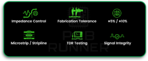
- High frequency PCB impedance control means holding a trace’s electrical resistance to fast-changing signals within a tight, specified range, usually ±5% or ±10% of the target value.
- Fabrication tolerances come from real-world variation in etching, lamination, and dielectric thickness. No process holds a trace dimension perfectly, which is why every impedance spec needs a stated tolerance.
- A standard impedance tolerance PCB build runs ±10%. Advanced or RF-grade builds tighten that to ±5%, and some differential pairs stay at ±10% even in advanced builds because of how broadside coupling behaves.
- Microstrip traces sit on an outer layer with one reference plane. Stripline traces run between two planes. Stripline holds tolerance more consistently but costs more to build and test.
- Every impedance-controlled board should ship with time-domain reflectometry (TDR) test data from a coupon, not just a simulation printout. For controlled-impedance builds, coupon-based TDR testing is commonly used to verify that the manufactured transmission-line structures meet the specified impedance tolerance.
- Getting this wrong shows up as signal reflection, data errors, or EMI failures, usually after the board is already assembled and in test.
A board can pass every visual inspection, look flawless under a microscope, and still fail on the bench because one trace is running six ohms off target. That single number is often the difference between a clean data eye and a board that won’t hold certification.
The stakes are only going up. The FCC has opened more than 13 GHz of millimeter-wave spectrum above 24 GHz for 5G, IoT, and satellite broadband services, and that spectrum runs through boards that have to hold their electrical behavior at frequencies most designers weren’t routing for a decade ago. High frequency PCB impedance control is what keeps a signal readable once it leaves the driver and travels down a trace instead of just sitting on a schematic.
This blog breaks down what impedance control actually is, why manufacturing tolerances exist in the first place, and what to check before you commit a board to production.
What Is High Frequency PCB Impedance Control?
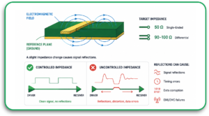
Impedance control is the practice of designing and building a trace so its electrical resistance to a changing signal stays within a set range, almost always centered on 50 ohms for single-ended traces or 90 to 100 ohms for common differential pairs.
Impedance control is the practice of designing and manufacturing a PCB transmission line so its characteristic impedance remains within a specified tolerance around the target value, commonly 50 Ω for single-ended traces and 90–100 Ω for many differential interfaces.
At low speeds, a trace behaves like a simple wire. At high frequencies, it stops acting like copper and starts acting like a transmission line. The signal travels as an electromagnetic field around the trace, not just current through it. If the trace’s impedance shifts even slightly along its length, part of the signal reflects backward instead of reaching the receiver.
That reflection causes:
- Signal reflections that distort the waveform
- Timing errors on high-speed digital buses
- Data corruption on serial links running above a few Gbps
- Radiated noise that can fail EMI/EMC testing
PCB Impedance Control is one of the few specs where “close enough” genuinely isn’t close enough. A trace 15% off target on a 10 Gbps link can be the entire reason a board fails validation.
Why Does Impedance Control Depend on Manufacturing Tolerances?
Impedance is calculated from trace width, copper thickness, dielectric thickness, and the dielectric constant of the laminate. None of those numbers come out of a fabrication line at exactly the value on the drawing. Etching removes a slightly different amount of copper on every panel. Laminate presses compress dielectric layers within a range, not a fixed point. Copper foil itself varies by a few tenths of a mil between rolls.
That’s where PCB Manufacturing Tolerances come in. A tolerance is the fabricator’s honest statement of how close the finished trace will land to your target, given the real variation in their process.
At PCB Runner, controlled impedance is built to two tiers:
| Impedance Type | Standard | Advanced |
| Single-Ended | ±10% | ±5% |
| Differential, Edge-Coupled | ±10% | ±5% |
| Differential, Broadside-Coupled | ±10% | ±10% |
A few things worth noticing in that table:
- Standard builds hold ±10%, which is fine for most digital interfaces running below a few Gbps.
- Advanced builds tighten single-ended and edge-coupled differential traces to ±5%, which is what most RF and high-speed serial designs actually need.
- Broadside-coupled differential pairs stay at ±10% even in advanced builds. That’s not a shortcut. Broadside coupling depends on dielectric thickness between two layers, and that dimension carries more inherent process variation than trace width does.
If your design calls out a tolerance tighter than what your fabricator can actually hit, you’ll get boards that pass incoming inspection but fail in the field. Confirm the number before you release the design, not after the first batch ships.
How Does Controlled Impedance Manufacturing Actually Work?
Controlled impedance manufacturing starts long before the first panel goes into etch. It’s a stack of decisions that all move the final number:
- Stackup design. The fabricator maps out layer count, copper weight, and dielectric thickness to hit the target impedance using field-solver software, not a spreadsheet formula alone.
- Material selection. Standard FR-4 works for moderate speeds. RF and high-frequency designs typically need low-loss laminates such as Rogers materials, which hold a more stable dielectric constant across frequency and temperature.
- Etch compensation. Copper etches from the sides as well as the top, so the fab adjusts the artwork slightly wider or narrower than the drawing to land on the finished target width.
- Panel-level verification. A test coupon travels alongside every production panel and gets measured before the boards ship.
Here’s a real pattern from the shop floor: a customer specs a 50-ohm single-ended trace for a high-speed board. The stackup is correct on paper. But the laminate batch used for that run has a dielectric constant running slightly higher than the datasheet nominal. Without in-process adjustment, the trace comes out at 44 ohms, outside a ±5% window. A fabricator running real coupon testing catches this before shipment and adjusts. One that skips testing ships boards that fail in the customer’s lab weeks later.
Here’s a real manufacturing scenario: a customer specifies a 50-ohm single-ended trace for a high-speed board. The stackup may be correct in the design model, but variations in finished trace width, copper thickness, dielectric thickness, and laminate properties can shift the manufactured impedance away from the target. Coupon-based TDR testing allows the fabricator to verify whether the completed production lot remains within the specified impedance tolerance before shipment.
Want the math behind how these numbers get calculated in the first place? PCB Runner’s guide on accurate impedance calculations in modern PCB design walks through the formulas step by step.
Microstrip vs. Stripline: Which Holds Tolerance Better?
Both are valid ways to route a controlled-impedance trace, but they behave differently and that difference affects tolerance.
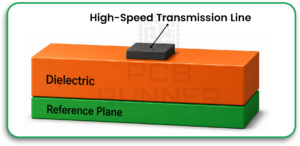
Microstrip
- Sits on an outer layer with one reference plane below it
- Easier and cheaper to fabricate
- More exposed to environmental effects like solder mask thickness variation
- Typically holds ±10% tolerance comfortably, ±5% with tighter process control
 Stripline
- Runs on an inner layer, sandwiched between two reference planes
- More consistent electrical environment since it’s shielded from surface variation
- Can hold tighter tolerance more reliably at high frequency
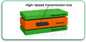
Microstrip stripline manufacturing choices usually come down to where the trace needs to live in the stackup and how much shielding the signal needs from external noise. RF front-end traces that need to stay isolated often go stripline. High-speed digital buses that need easy probing during debug often stay microstrip.
Where Does Tight Impedance Tolerance Actually Matter?
Not every board needs ±5%. Here’s where it genuinely does:
- 5G and RF front-end modules, where mismatched impedance directly reduces transmitted power and range
- Medical imaging and diagnostic equipment, where signal timing errors can produce inaccurate readings
- Aerospace and defense radar systems, where a reflected signal can look like a false target
- High-speed data center and networking gear, where serial links running above 10 Gbps have almost no margin for reflection
- Automotive radar and ADAS modules, where the operating frequency has pushed well into the tens of GHz
If your board doesn’t touch RF, doesn’t run high-speed serial protocols, and doesn’t need certified timing accuracy, a standard ±10% build is often the right call and the more cost-effective one.
What Should You Check Before Ordering an RF or High-Speed Board?
Before releasing a design for high frequency PCB impedance control, confirm these with your fabricator:
- What tolerance can they actually hold, not just what they advertise. Ask for recent coupon data on a similar stackup.
- What laminate they’re proposing and whether its dielectric constant is stable across your operating frequency range.
- Whether they test every panel with TDR, or only sample a batch.
- How they handle broadside-coupled pairs, since that tolerance often stays looser than single-ended traces.
- Turnaround time for impedance-controlled builds, since these boards usually take longer than standard multilayer runs due to the extra verification step.
A quick way to sanity-check your own design before you send it out: review PCB Runner’s impedance page, which lists the exact tolerance bands used in production, so you can match your spec to a tolerance that’s realistically achievable.
How Is Impedance Testing PCB Verified After Fabrication?
Impedance testing PCB verification happens two ways, and a serious fabricator uses both.
Time-domain reflectometry (TDR) sends a fast step signal down a test trace and measures how it reflects. Any point where impedance changes shows up as a spike in the reflection, which pinpoints exactly where a trace drifts out of spec.
Test coupons are small strips of the same stackup, etched alongside the production panel using the same materials and the same process run. Measuring the coupon tells you what the actual boards in that batch look like, not what a simulation predicted they’d look like.
If a supplier can’t produce TDR data for your specific order, that’s worth asking about directly before production starts.
What Does Impedance-Controlled Fabrication Cost?
Impedance control adds cost, and it’s worth knowing where that cost comes from instead of treating it as a flat markup:
- Engineering time to model the stackup and hit the target before production starts
- Test coupon production and TDR measurement on every panel or lot
- Material cost, since low-loss RF laminates cost more than standard FR-4
- Lower panel yield, since tighter tolerance sometimes means smaller usable panel area
- Longer lead time, since verification adds a step that standard boards skip
The tighter the tolerance, the more of these costs stack up. A ±5% advanced build typically costs more than a ±10% standard build on the same layer count, but it’s the difference between a board that works at 10 GHz and one that doesn’t.
FAQs
Q. What’s the difference between impedance and resistance on a PCB trace?
Resistance is a fixed value that doesn’t change with signal speed. Impedance is what a trace presents to a fast-changing signal, and it depends on trace geometry, the dielectric material, and frequency. At high speed, impedance is what actually determines whether your signal arrives intact.
Q. Can I get ±5% tolerance on every layer of my board?
Usually yes for single-ended and edge-coupled differential traces on an advanced build. Broadside-coupled differential pairs are the exception; most fabricators, including PCB Runner, hold those at ±10% because of how dielectric thickness variation affects that specific coupling type.
Q. Do I need Rogers material for a high-frequency board, or will FR-4 work?
It depends on your frequency and loss budget. Standard FR-4 can work up into the low GHz range for less demanding designs. Once you’re pushing RF frequencies or need very stable dielectric behavior across temperature, low-loss laminates like Rogers become the safer choice.
Q. How do I know if my design actually needs controlled impedance at all?
If you’re routing single-ended signals below a few hundred MHz with generous timing margin, you may not need it. If you’re running differential pairs, RF signals, or serial links above roughly 1 Gbps, controlled impedance stops being optional.
Q. Will tighter tolerance slow down my order?
Yes, typically. Advanced impedance builds need extra engineering review and coupon testing, which adds days compared to a standard build. It’s worth building that into your project timeline rather than finding out at the quote stage.
Ready to Lock In Your Impedance Tolerance?
Getting high frequency PCB impedance control right starts with an honest tolerance spec and a fabricator who tests every panel instead of trusting simulation alone. If you’re working on an RF, high-speed digital, or radar design and want a stackup review before you commit to production, request a quote from PCB Runner and share your target impedance, layer count, and frequency range. Our team will confirm what tolerance we can actually hold on your build before you place the order.



