


Objective
Show process engineers and PCB buyers how stencil aperture design directly causes or prevents the two most common solder paste printing defects, bridging and insufficient solder, so they can spot the problem before a bad batch reaches reflow.
Key Takeaways
- Solder paste printing defects cause an estimated 60 to 70 percent of all SMT assembly defects, more than any other step in the process.
- Bridging usually traces back to oversized apertures, low area ratio, or pads placed too close together without a mask dam.
- Insufficient solder paste is almost always an aperture problem: too small, too thick a stencil, or a clogged wall that won’t release paste.
- IPC-7525 sets two hard numbers to check before you approve a stencil: area ratio of 0.66 or higher, aspect ratio of 1.5 or higher.
- SPI inspection catches these defects before placement, when a board just needs a wipe and a reprint instead of expensive rework.
A board comes off the reflow oven, AOI flags six shorts on the same QFP, and now someone has to figure out whether it’s a placement issue, a reflow profile issue, or something further upstream. Nine times out of ten, it started at the stencil.
Solder paste printing happens before any component touches the board, and it sets the ceiling for how good the finished assembly can be. Industry data puts the number bluntly: somewhere between 60 and 70 percent of SMT defects trace back to this one step. Get the stencil wrong and every downstream process, placement, reflow, inspection, is just working around a problem that already exists.
This piece breaks down the two defects that show up most often, bridging and insufficient solder, and shows exactly where in stencil design each one starts.
What Are Solder Paste Printing Defects?
Solder paste printing defects are print-stage errors in how much paste lands where it’s supposed to, before any component gets placed. The paste itself is a mix of tiny metal solder balls suspended in flux, and a stencil squeegees it through cut openings onto the pads below.
When that transfer goes wrong, you get one of a short list of repeat offenders:
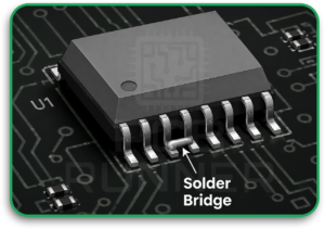
- Bridging – paste connects two pads that should stay separate
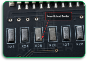
- Insufficient solder – too little paste lands on a pad, or none at all
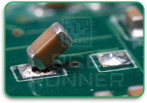
- Tombstoning – uneven paste volume lifts one end of a small component during reflow
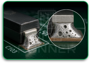
- Voiding – trapped gas pockets inside a solder joint after reflow
The first two, bridging and insufficient solder, account for most of the rework tickets on a typical SMT line. Both come from the same root cause more often than people expect: the stencil.
What Causes Solder Bridging?
Bridging happens when solder connects two adjacent pads that were never meant to touch, usually showing up as a short circuit after reflow. It’s almost always a print-stage problem, not a placement problem.
The usual suspects:
- Oversized apertures. If the cutout is wider than the pad needs, excess paste squeezes out sideways during the print stroke and touches the next pad over.
- Low area ratio. IPC-7525 recommends keeping the area ratio (opening area divided by wall area) above 0.66. Below that, paste sticks to the aperture walls instead of releasing cleanly, and what does release comes out uneven, some pads flooded, some starved.
- Insufficient pad-to-pad spacing. Fine-pitch parts like 0.4 mm QFNs and BGAs leave almost no margin. Without a proper mask dam between pads, there’s no physical barrier stopping solder from spreading.
- Board flex during the squeegee stroke. A board that bows even slightly lets the stencil lift off the surface in spots, and paste seeps under the gap.
- Wrong squeegee speed or pressure. Too slow, and paste overfills wide apertures. Too much pressure, and paste smears past the aperture edge before it releases.
Fine-pitch QFPs and BGAs with 0.4 to 0.5 mm pitch are the parts most likely to bridge, simply because there’s almost no room for error at that spacing.
What Causes Insufficient Solder Paste?
Insufficient solder paste is the opposite failure: a pad gets too little paste, or none, which leads to weak joints, opens, or the dreaded head-in-pillow defect on BGAs where the ball never fully wets to the pad.
Common causes:
- Undersized apertures. Reducing an aperture too aggressively to fight bridging on one side of the board can starve paste volume on the other.
- Clogged aperture walls. Old paste residue, moisture, or a rough-cut stencil wall keeps fresh paste from releasing fully.
- Stencil too thick for the pitch. A 0.15 mm stencil works fine for standard components but chokes paste release on 0.4 mm pitch parts, where a thinner 0.10 mm stencil is usually the better call.
- Low area ratio, same root cause as bridging. It’s worth repeating: a bad area ratio doesn’t just cause one defect. It causes inconsistent paste release across the board, which means some pads bridge and others come up short in the same print run.
- Worn or damaged squeegee blade. A nicked or worn blade skips paste unevenly across the stencil surface.
This is the part that trips people up: bridging and insufficient solder often come from the exact same stencil flaw. Fix the area ratio, and you often fix both problems at once.
How Does Stencil Design Actually Prevent These Defects?
Good stencil design isn’t guesswork. IPC-7525 gives two specific numbers to check before a stencil ever goes into production.
Area ratio measures aperture opening area against the wall surface area inside that opening. IPC-7525 sets the floor at 0.66. Stay above it, and paste releases cleanly onto the pad. Drop below it, and paste clings to the walls, causing exactly the volume inconsistency that drives both bridging and insufficient solder.
Aspect ratio compares aperture width to stencil thickness. The minimum is 1.5. Fall short, and the walls dominate the opening enough that paste can’t transfer reliably no matter how good the area ratio looks on paper.
Beyond the two ratios, a few design choices make a measurable difference:
- Aperture reduction for fine pitch. Standard practice trims apertures 5 to 20 percent smaller than the pad itself on fine-pitch parts, which limits volume without starving the joint.
- Trapezoidal or home-plate apertures. A slightly narrower opening at the bottom than the top helps paste release cleanly instead of clinging to vertical walls.
- Window-pane apertures for thermal pads. Large QFN and BGA thermal pads get split into a grid of smaller openings instead of one big cutout, which improves release and cuts down on trapped voids.
- Stencil thickness matched to the smallest pitch on the board. A single stencil thickness rarely suits every component. Step stencils, thicker in some zones and thinner in others, solve this when a board mixes standard and fine-pitch parts.
- Laser-cut apertures with smooth wall finish. A rougher cut wall from an older-generation stencil process holds onto more paste than a clean laser-cut edge, which quietly hurts area ratio performance even when the numbers on paper look fine.
None of this replaces good reflow profiling or careful placement. But if the stencil delivers the wrong paste volume in the first place, nothing downstream can fully correct it.
What Role Does SPI Inspection Play?
SPI inspection (Solder Paste Inspection) checks paste volume, height, area, and alignment on every pad right after printing, before any component gets placed. This is the cheapest point in the whole process to catch a defect.
Here’s why the timing matters so much. A board with bad paste print, at this stage, just needs a clean and a reprint. Once that same board goes through placement and reflow, a defect turns into a rework job, and if it slips through to the field, the cost multiplies again.
Modern 3D SPI systems measure actual paste volume rather than just checking that a deposit looks roughly the right shape from above. That distinction matters more than it sounds. A deposit can look correct from a 2D camera and still be 30 percent short on volume, which shows up later as a cold joint nobody predicted from the print stage alone.
SPI data also feeds back into process control. Tracking paste volume trends over a production run flags a wearing squeegee blade or a stencil going out of alignment before defect rates climb, not after.
How Do You Troubleshoot a Stencil That’s Already Causing Problems?
If a specific pad or component keeps showing bridging or insufficient solder across multiple boards, work through this order:
- Pull the SPI data for that pad location. Check whether the volume trend shows consistent under-fill, over-fill, or random variation. Random variation usually points to a release problem, area ratio or wall roughness.
- Recalculate the area ratio for that specific aperture. Confirm it against IPC-7525’s 0.66 minimum using the actual aperture dimensions and stencil thickness, not the numbers from the original design file if the stencil has been in service a while.
- Inspect the aperture walls under magnification. Look for paste buildup, corrosion, or a rough cut edge that wasn’t visible at first glance.
- Check squeegee condition and pressure settings. A nicked blade or inconsistent pressure produces the same symptoms as a stencil design flaw, so rule this out before redesigning anything.
- Confirm board support during the print stroke. A board that isn’t fully supported can flex just enough to cause localized lift-off, even on an otherwise correct stencil.
If the ratios check out and the equipment is in good shape, the problem often comes down to component footprint itself, meaning the pad layout on the PCB needs adjusting, not just the stencil.
Conclusion
Getting the stencil right the first time saves far more than a reprint. It’s the difference between a clean first-pass yield and a stack of boards headed for rework. If you’re seeing repeat bridging or insufficient solder on a current build, PCB Runner‘s assembly team reviews stencil design and DFM files against IPC-7525 before your project goes to print, at no charge. Request a free quote.
FAQs
Q. What’s the difference between solder bridging and tombstoning?
Bridging connects two pads that shouldn’t touch, causing a short. Tombstoning is when uneven paste volume on a small two-terminal part, like a resistor or capacitor, pulls one end up off the board during reflow. Different defects, but both often start with inconsistent paste volume from the stencil.
Q. Can a good reflow profile fix a bad stencil print?
No. Reflow can’t add paste volume that wasn’t printed, and it can’t undo excess paste that’s already bridging two pads. The print stage sets a ceiling on joint quality that reflow settings can’t raise.
Q. How often should stencils be cleaned or replaced?
Cleaning frequency depends on paste type and print volume, but most lines clean the underside every few prints and do a full wipe-down at set intervals during a run. Replace a stencil once aperture walls show visible wear, corrosion, or damage that affects release.
Q. Is a thinner stencil always better for fine-pitch parts?
Generally yes for pitch below 0.5 mm, since thinner stencils improve the aspect ratio. But go too thin across a whole board and you’ll starve paste volume on larger, standard-pitch components. This is exactly why step stencils exist for mixed-pitch boards.
Q. What information do I need to give a PCB assembler to avoid these defects?
Accurate Gerber files with the paste layer included, a BOM with correct component pitch and package data, and any known problem areas from previous runs. A capable assembler will review stencil design against IPC-7525 before printing the first board, not after defects show up.



