DFMA for PCBs

DFMA for PCBs: Key Elements in Design and Assembly Efficiency

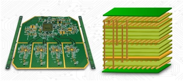
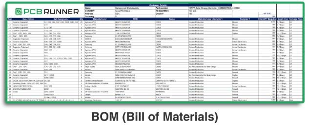
As in most industries, electronic markets require the PC board assembly to be as optimized as possible for cost, reliability, and overall production workflow. This is where the Design for Manufacturing and Assembly (DFMA) principles kick in. DFMA is a systematic method that contains design instructions that guide the assembly of circuit boards and components in ways that minimize time and costs.

Integrating DFMA for PCBs enables designers and manufacturers to improve product quality while reducing assembly time and material costs. The idea is to achieve a balance between manufacturability, assemblability, functionality, and reliability. In this blog post, I will discuss the DFMA principles for PCBs, their influence on production, and the reasons why they are needed in optimized electronic products.

Defining DFMA in PCB Design

What does DFMA mean?

There are two key components of DFMA. 

  1. Design for Manufacturing (DFM): Deals with the design approach toward multilayer PCBs and other board types to maximize ease of fabrication and minimize production costs.
  2. Design for Assembly (DFA): Deals with assembly-related issues where there is a large number of different parts by reducing the number of parts to be assembled, incorporating standardized components, and simplifying the layout of the wiring board.

With these two strategies combined, DFMA for PCBs will assist in eliminating manufacturing mistakes, shortening production times, and increasing product strength. 

Important DFMA Considerations For PCBs

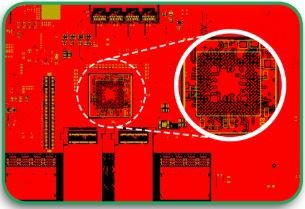
1. Optimization of the PCB Structure

Complex circuit board assemblies significantly increase cost and the possibility of defects. When optimizing PCB fabrication, designers should: 

  • Stand operate board shapes to eliminate additional material cutting and wasting.
  • Eliminate unnecessary layers in multilayer PCBs.
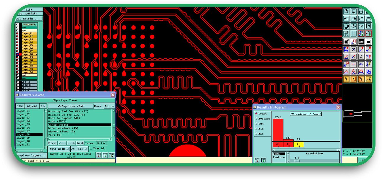
  • Organize and physically separate trace routing to aid in testing and debugging procedures.
  • Eliminating features doesn’t add much to the overall cost of manufacturing and production time.

Optimization of the PCB Structure

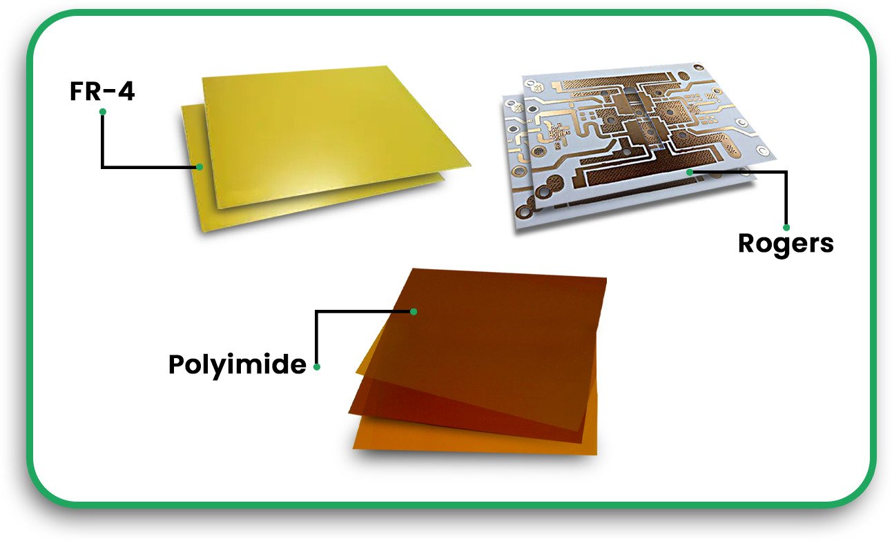
2. Utilize Appropriate Components and Materials

Using commercially available components can increase the efficiency of the PCBs remarkably. Using off-the-shelf items does have some limitations. Considerations include: 

  • Non-custom components that greatly reduce procurement expenses.
  • Component footprints that do fit with standard DFMA when designing the PCB. 

By using readily optimized materials and components, production time greatly increases since the risks are greatly mitigated.

Utilize Appropriate Components and Materials_

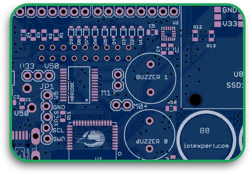
3. Making PCB Layouts More Assembly Friendly

There is no doubt a good PCB layout will enhance the effectiveness of the pc board assembly. Here are some tips the designers can follow to achieve this:

  • Position high-frequency components near the connectors in order to reduce interference.
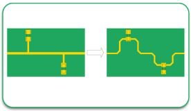
  • In multilayer PCBs, vias should be kept to a minimum to increase reliability.
  • Allow sufficient spacing between components for automated assembly machines.
  • Other activities like testing and troubleshooting become easy when the layout is optimized.

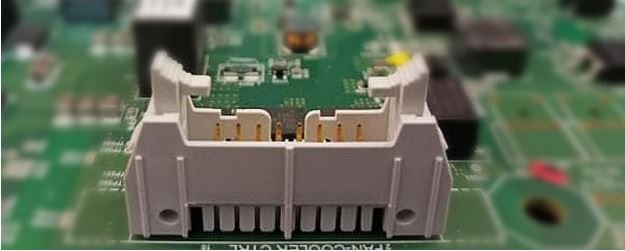
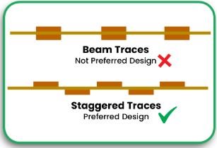
4. Cuts on Connected Flexible Parts

Flexible circuits do have their place within the industry, but an overabundance can hinder the ease of assembly when it comes to the printed circuit board. In order to promote reliability:

  • Use rigid connectors in place of weak ribbon cables.
  • Reduce interconnects and connectors to lower failure rates.
  • Design the PCB to allow for surface-mount devices, which eases automated assembly.
  • Incorporating single-sided PCBs for flexible areas while doing away with any fragile segments increases the durability of the end product.

Cuts on Connected Flexible Parts

PC Board DFMA Assembly, Making It More Efficient

1. PC Board Assembly Automation

A significant portion of assembly on a pc board is done automatically. DFMA for PCBs promotes the utilization of the following:

  • “Pick-and-place” machines make the placement of board components both faster and more accurate.
  • Reflow and wave soldering allows for automated soldering.
  • Assembly defects are detected at an early stage with automated optical inspection (AOI).

The incorporation of automation during the PCB design process leads to increased consistency while lowering labor costs.

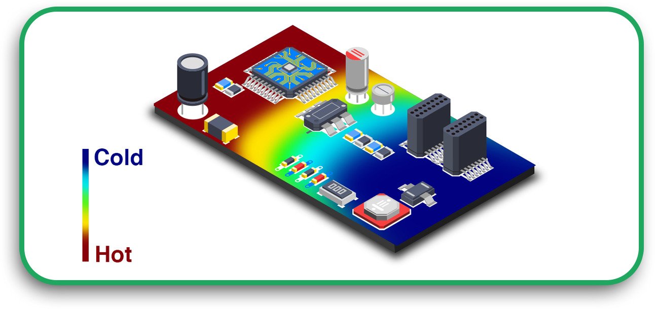
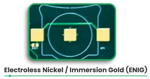
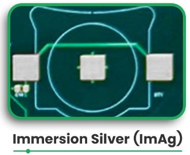
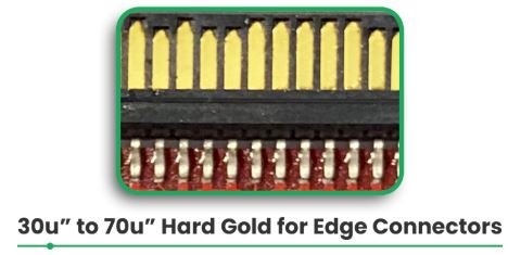
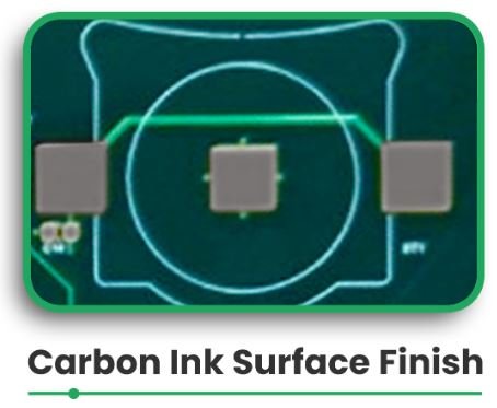
2. Proper Application of a Solder Mask

A solder mask on a PCB prevents the soldering-related bridges while at the same time protecting the copper traces from oxidation. When using the DFMA technique, it is best to remember the following:

  • Select a solder mask material that can endure high temperatures, as well as chemical contact.
  • Apply solder mask layers sufficiently to achieve proper coverage.
  • Maintain spacing clearance between pads and apertures to enable zero short-circuit occurrences.

Performance and deterioration of the PCB can be enhanced by having a properly applied solder mask material.

3. Consolidating Assembly Operations

According to the DFMA rules, in order to increase efficiency of assembly operations:

  • Eliminate components that are different in type to make stock control simpler, as well as to reduce manipulation.
  • Employ similar standards in attaching equivalent components.
  • Where feasible, incorporate parts to reduce the number of different assemblies.

Adhering to these steps leads to reduced production time, as well as lower economic costs.

Benefits of DFMA for PCB Manufacturers

  1. Cost Savings

  • Reducing unnecessary complexity in PCB design lowers production costs.
  • Standardizing components allows for bulk purchasing and reduces expenses.
  1. Improved Product Reliability

  • Fewer interconnections and simpler layouts minimize potential failure points.
  • Optimized solder mask material application enhances protection against environmental factors.
  1. Faster Time-to-Market

  • Streamlining manufacturing and assembly reduces production delays.
  • Minimized revisions ensure that PCBs are ready for use more quickly.
  1. Higher Manufacturing Efficiency

  • Automated assembly compatibility speeds up the production process.
  • Clear design guidelines reduce errors and improve consistency.

Best Practices of DFMA and Emerging Business Developments

The Growing Power of The Small Device

More powerful, smaller devices mean increased demand for higher performance and more compact multilayer PCBs.

The balance achieved between assembly ease and deep miniaturization exemplifies distinctions in DFMA principles.

An Increasing Need for Dependable Electronics

Automotive, aerospace, and medical sectors have more stringent designs for manufacture and assembly requirements for PCBs.

Quality control has become the number one priority for PCB circuit board manufacturers.

Expansion Tech of AI and Automation in Industry

In PCB design, AI-powered DFMA software adjusts the layout for speed and other factors.

Monitoring and testing become automated, removing the need for manual quality assurance.

Expert Insight

By integrating digital fabrication (Dfab) and design for additive manufacturing (DfAM), DfMA streamlines the construction process, making it more precise and sustainable.

A review of 171 research articles highlights key aspects of DfMA, including its fundamental principles, its role in Dfab and DfAM, and its application in additive manufacturing (AM) assembly. Additionally, the potential of machine learning in optimizing DfMA processes has been explored, revealing significant opportunities for automation and efficiency.

Despite these advancements, there remain notable research gaps in DfMA for Dfab and DfAM. Addressing these gaps could enhance operational performance, reduce material waste, and support more sustainable construction practices. As the industry continues to evolve, further research and innovation in DfMA will be essential for shaping the future of construction.

Conclusion

To enhance reliability, lower costs, and optimize pc board assembly and construction administration, applying DFMA techniques for PCBs is critical. The simplification of design, selection of solder mask, and reduction of steps in assembly all serve to increase production effectiveness.

With the multifunctional capabilities of PCBs, they are faster to design alongside assembly integration and the process as a whole. Thus, time-to-market is lessened, and product quality is improved.

At PCB Runners, we offer professional assembly services and circuit board manufacturing. Call us today so we can assist you in improving your PCB production processes and for greater savings without compromising quality standards!

FAQs

What is DFMA in PCB manufacturing?

Within the scope of PCB manufacturing, DFMA (Design for Manufacturing and Assembly) is the approach that optimizes the design process by making it easier to manufacture and assemble the product.

Why is DFMA important in circuit board assembly?

It simplifies the construction and assembling processes of the circuit board in a way that standard components can be suitably integrated within.

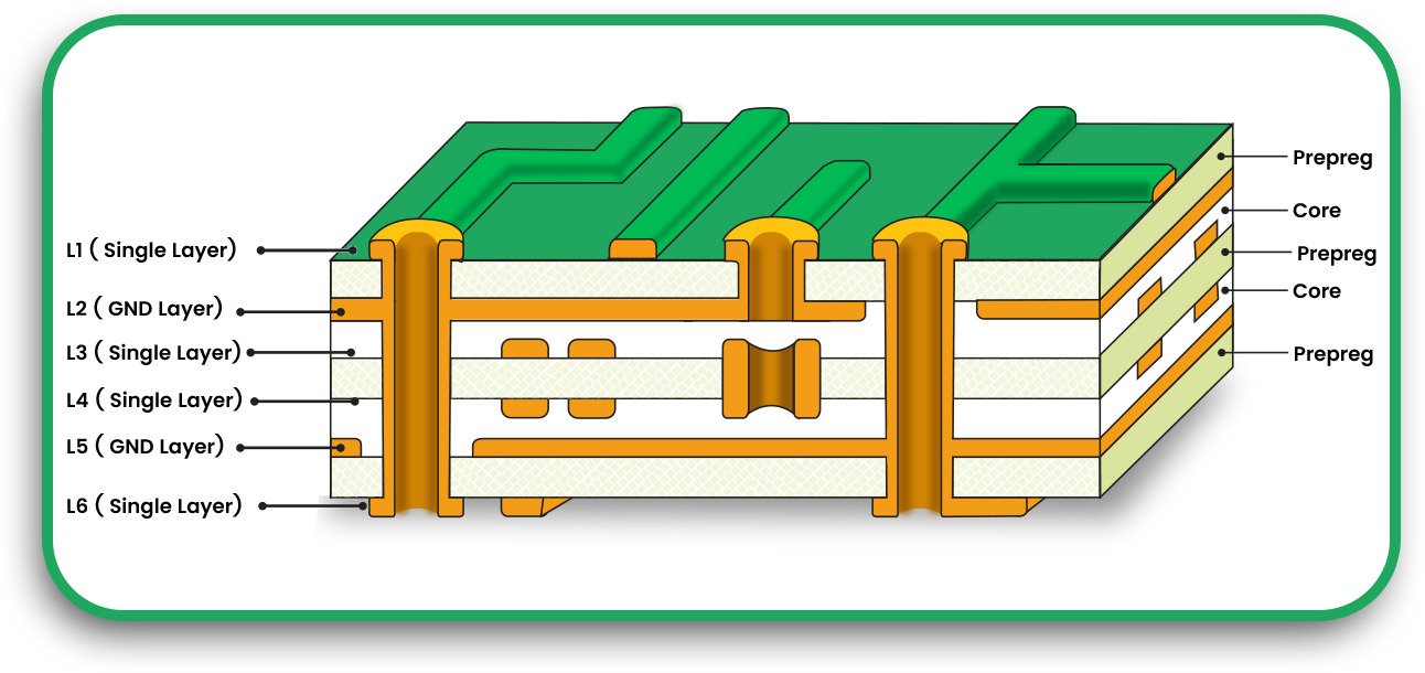
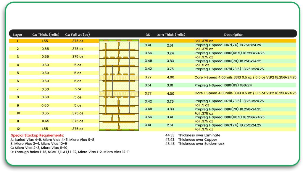
How does DFMA impact multilayer PCBs?

Cost reduction is the most obvious advantage of adopting multilayer technology. Most stack-up designs are optimized for performance, reliability, electrical integrity, and ease of manufacturability.

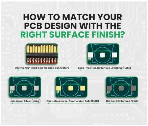
What role does solder mask material play in DFMA?

The best solder masks prevent the exposure of the copper circuitry to oxygen in the environment. These aids in avoiding PCB oxidation, prevents short circuits, and make the circuit board more robust.

How can PCB Runners help with DFMA-compliant PCB design?

With PCB Runners, you are assured that your boards will be assembled with care and accuracy. We employ strategies that are cost-effective while ensuring the highest quality in PCB assembly.

The Role of PTH Technology in High-Reliability PCB Designs

These days, almost every electronic device uses a printed circuit board (PCB). New technologies are constantly emerging, and with them, the demand for advanced PCBs rises, particularly in the aerospace, telecom, and medical device sectors.

One of the most commonly used technologies for achieving strong and durable connections is the Plated Through-Hole technology (PTH).

This article compares PTH technology with other advanced methods of making custom-printed circuit boards, such as HDI circuit boards and their PTH counterparts. It also details the key features of custom-printed circuit boards and their durability with PTH technology.

PTH Technology in High-Reliability PCB Designs

What is PTH Technology?

With PTH Technology, an entire PCB assembly is utilized, where holes are drilled through the board and plated with a specific metal to create sturdy electrical connections between the board layers. This type of assembly allows for proper soldering of leads through the board using components equipped with leads.   

How PTH Works

Drilling: The PCB is drilled with mechanical drills that create precise holes.

Plating: The inside walls of the holes are coated with conductive materials like copper.

Insertion of Components: Components with leads are placed through sufficient holes.

Soldering: A soldering iron is used to solder the leads for a secure connection both electrically and mechanically.

Types of PTH PCBs

Single-Sided PTH PCB: This is used in basic circuit designs only.

Single-Sided PTH PCB
Double-Sided PTH PCB: The components are placed on both sides of the board, increasing the circuit’s complexity.

Double-Sided PTH PCB

Multi-Layer PTH PCB: Enhanced features with multiple interconnected layers for a complex, highly efficient multifunctional task.

The Merits of PTH Technologies

Durable Connections: Ideal in applications with high stress, these connections are mechanically rigid and have reliable electrical contact.

Multi-layer Interconnects: Allows for the effortless interconnection of different layers of a custom printed circuit board and its components.

Superior Heat Endurance: Endure highly high temperatures which are prevalent in the industrial and automotive sectors.

Dependable In-Higher Current Applications: Superior current bearing capability in comparison to surface-mounted devices.

Easy Assembly: Suitable for wave soldering and other forms of automation soldering processes.

PTH Technology vs. HDI Circuit Boards

While PTH technology has been a standard for years, High-Density Interconnect (HDI) circuit boards offer an alternative for modern miniaturized electronics.

Key Differences

Feature PTH Technology HDI Circuit Boards
Connection Type Plated through-hole Microvias & blind/buried vias
Board Density Lower Higher (supports compact designs)
Electrical Performance Standard Enhanced signal integrity
Manufacturing Cost Moderate Higher due to advanced processes
Reliability Excellent for high-stress applications Ideal for lightweight, high-speed devices

Choosing between PTH and HDI

For military, aerospace and industrial electronics, choose PTH PCB boards as they are built to sustain extreme conditions.

For consumer electronics, smartphones, and other devices with space constraints, consider using HDI circuit boards.

Expert Insight

With the increase in the complexity of PCB designs, more factors need to be considered apart from conventional PTH processes. An obstacle that has emerged is the mechanical drilled hole size and plating aspect ratio, which could reduce routing density. To achieve high feature density, PCB fabricators focus on enabling all-in-ravaged capabilities with laser micro vias, blind and buried vias, and stacked micro vias. These techniques improve design flexibility and signal integrity.

Thermal cycling and reliability are other key factors. Exposed PTH solder joints have to bear the stress of heat expansion and contraction cycles, which significantly affects their reliability. To reduce the impact of these issues, improved plating processes and innovative materials ensure long-term durability in harsh conditions.

Uses of PTH PCB Boards

  1. Aerospace and Defense
  • Provides exceptional reliability in harsh environments.
  • Endures physical vibration shocks.
  • Covers vital avionics and radar systems.
  1. Medical Devices
  • All needed electrical connections are sustained over extended periods in lifesaving devices.
  • Resistant to harsh surroundings and sterilization procedures.
  • Applied to MRI machines, pacemakers, and some diagnostic equipment.
  1. Automotive Electronics  
  • Sustains high temperature and vibration experienced in vehicles.
  • Controls power management and engine control units.
  • Supports ADAS.
  1. Industrial Equipment
  • Allowed the development of harsh designs for factory automation.
  • Applied in the distribution of power and the operation of heavy equipment.
  • Guarantees dependability within severe industrial conditions.
  1. Consumer Electronics
  • Guarantee reliability for the home electronic devices and video gaming systems.
  • Applied in audio systems, televisions, and other smart appliances.

Engineering Considerations for PTH Technology

Hole Size and Aspect Ratio: Ensuring that the ratio enhances the conductivity and the mechanical strength.

Plating Thickness: Sufficient thickness of copper in the drillable region to withstand electrical gaps and make sure that there is no failure.

Signal Integrity: By making a good layer stack up and placing the vias in the correct positions, we do not allow for any electrical contaminations between the different levels.

Future of PTH Technology

As crucial as PTH technology is for high-reliability uses, developments in HDI circuit boards and the via-in pad technique certainly herald a new era in PCB manufacturing. Engineers are increasingly inventing hybrid designs that use a combination of PTH and HDI technologies to achieve an optimal balance of reliability, performance, and cost.

New Innovations in PCB Design and Manufacturing

Use of Novel Materials: New substrates that provide better strength.

More Effective Plating: Increasing the strength and conductivity of the board.

Manufacturing Automation: Improving accuracy and decreasing the cost of the processes.

Hybrid PCBs: The use of the two methods to achieve the best results.

Final Remarks

The importance of PTH technology in the manufacturing of custom-printed circuit boards cannot be overstated; it is the most dependable technology with the greatest effectiveness in high-stress situations.

PTH PCB boards remain the preferred option in industries where long-term durability and performance are critical, even though limited compact designs are beneficial in HDI circuit boards. Appreciating the merits of each technology enables PCB fabricators to design PCBs that meet the requirements of different applications and industries.

Are you looking for a supplier that can produce PCBs with a highly reliable design? Contact us today, and let us help you with your electronic requirements.

Optimizing PCB

Optimizing PCB for Efficient Electronics Design

The development of devices that are deeply integrated with modern technology begins with PCBs. Hence, Printed Circuit Boards and their designs are necessary to create a low-cost, high-performance product that is reliable in the long term. Custom PCBs are made to cater to varying industry needs, from consumer-based electronics to industrial-grade machinery. 

The emergence of PCBs with software-based electronic circuits has made it possible for designers to design more efficient, compact, and powerful PCBs. This article examines the critical issues with regard to the optimization of electronic PCBs from layout design, material choice, signal integrity, and even thermal management.

Important Aspects in PCB Optimization

1. Trace Length and Positioning Design

The layout is key to reducing trace length and increasing overall performance. The right placement of components improves signal delay and minimizes interference and overall performance. This includes:

  • Trace Grouping: If the components are grouped, the trace length will be reduced significantly.
  • Trace Composition: Grouping signals can be improved by applying differential pair and shortest distance routing.
  • Power and Ground Planes: When power and ground layers are allocated, currents are more effectively distributed, and electromagnetic emissions are also minimized. 

Trace Length and Positioning Design_

2. Choosing the Best Material

The mechanical aspects of the PCB, such as thermal conductivity, signal durability and strength, and transmission, are very reversible. Here are some common materials used:

  • FR-4: The industry standard for PCBs. Socioeconomically beneficial. Good electrical performance.
  • Polyimide: Ideal material for flex PCBs because of its flexibility and heat resistance.
  • Rogers Laminates: Employed in non-microwave frequencies because of its low signal attenuation.

Choosing the Best Material_

3. Signal Integrity Issues and High-Speed Design

Signal integrity needs to be maintained in high-speed PCBs to avoid blurring and information loss.

  • Impedance Matching: Guarantees no reflection or loss of signals.
  • Crosstalk Reduction: Adequate space between traces reduces unwanted signal interference.
  • Shield and Ground: Proper grounding of devices reduces EMI problems.

signal integrity

4. Thermal Management

Great care must be taken to control heat, as uncontrolled heat buildup can cause severe component damage.

  • Heat Sinks and Vias: Aid in drawing away heat from critical components.
  • Thermal Pads and Conductive Adhesives: Improve the transfer of heat to the cooler parts.
  • Component Positioning: Positioning of heat-producing components helps to reduce excessive localized heating.

Thermal Management_

5. Multi-Layer PCB Design

In complex designs, the use of multi-layer PCBs has the following advantages:

  • Decrease in PCB Area: Increases the number of components usable in a limited area.
  • Increased Signal Strength: The use of separate layers for power and signal improves the performance.
  • Improved Reliability: Reduces the number of external connections and, therefore, removes potential points of failure.

Multi-Layer PCB

Expert Insight

The PCB assembly line’s optimization is now one of the most critical elements in balancing costs and achieving maximum output. The use of automated pick-and-place systems in PCB production makes it possible to automate many processes, thus minimizing manual mistakes and enhancing production rates. With the escalating sophistication of custom boards and the ever growing assortment of parts, these automated systems optimization has become a challenge, though.

Now, circuit designer software’s PCB assembly algorithms for electronic circuit design incorporate optimization of the placement of components for assembly. This algorithm relieves robotic arms of extra travel by cutting the time and number of movements needed for the pick-and-place operation processes. Research suggests that the efficiency of component placement is maximized if the number of components placed in a single movement is restricted to four. On the other hand, new designs of electro-pneumatic arms are anticipated to enhance the accuracy and speed of breakthrough PCB assembly instrumentation, which could be patentable.

The Importance of Software in PCB Optimization

Software Selection Guide

Using the correct software for electronic circuit PCB design makes the design process more straightforward and improves precision. Some of the leading ones include:

  • Altium Designer: Highly regarded for excellent simulation tools and collaborative editing in real-time.
  • Eagle PCB Design: Easy to use with a well-developed user base.
  • KiCad: Best for designers not working commercially since the software is open-sourced.
  • OrCAD: Best suited for more advanced circuit simulations and PCB layouts

What to Look For

When optimizing the design of a PCB, software should provide the following:

  • Auto-routing features: Aids to quickly place traces.
  • Thermal analysis: Ensures that overheating problems do not occur.
  • 3D visualization: Helps designers to see the final look of the board prior to fabrication.

Best Practices for PCB Manufacturing

DFM (Design For Manufacturing)

The principles of DFM guarantee that PCBs are manufactured and assembled easily. It includes the following:

Standard Component Sizes: The use of readily available parts facilitates easier procurement and assembly.

Vias: Cut unwanted costs and minimize potential weak points.

Silkscreen Marking: This makes the silkscreen more visible and legible to the assembly technicians.

Testing and Prototyping

Thorough testing must be done before the product goes into mass production:

Prototyping: Make it possible to catch mistakes in the design before they are too costly to address.

Automated Optical Inspection (AOI): Find solder defects, misalignments, and some other issues that are difficult to see with the naked eye

Electrical Testing: Check continuity and the quality of signals.

Trends For The Future in PCB Optimization

1. Automated PCB Design

To assist manual PCB designers, AI is set to be implemented into electronic design PCB CAD tools to automate design optimization and identify and rectify poor designs.

2. PCBs Made Using 3D Printing

The development of additive manufacturing is allowing for quicker prototypes and new, complex PCB designs that were unachievable through previously used methods.

3. Flexible and Wearable Electronics

As the need for flexible electronics increases, PCBs incorporating stretchable and bendable materials are serving the healthcare and smart textiles markets.

Conclusion

In the context of custom printed circuit board design, achieving efficiency and high performance in electronic devices requires a keen focus on detail. Engineers should use dedicated electronic circuit PCB design software to focus on layout, signal integrity, and thermal management. At the same time, manufacturers should emphasize design for manufacturability to improve productivity and cut costs.

Are you in need of professional PCB design and manufacturing services? Contact PCB Runners now to get solutions that fit your specifications!

PCB Layout Design for Electromagnetic Compatibility: A Guide for Optimal Performance

Every electronics industry professional today understands the requirement of a reliable PCB design that meets EMC standards. To keep up with the power and compactness of new devices one must keep in mind the risk of electromagnetic interference (EMI) that can truncate the overall performance. 

Thus, every PCB manufacturer or designer must tackle the challenges of an interference-free operation while designing the PCB layout, which is critical to a PCB design achieving EMC standards.

This blog will discuss the key principles of electromagnetic compatibility and offer tips to manage EMI and overall performance. It is crafted not only for seasoned PCB manufacturers but also for designers aiming to polish their skills in creating layouts and meeting EM standards.

PCB Layout Design for Electromagnetic Compatibility

Why Electromagnetic Compatibility Matters in PCB Design

A PCB is always designed with certain electronic components. Thus, electronic interference and electromagnetic noise are always monitored. A power supply must provide a reliable and smooth output without interference from external systems and devices.

In the context of PCB layout design, poor EMC design can lead to:

  • Undesirable signal interference.
  • Unwanted crosstalk.
  • Not achieving set regulatory standards.
  • Additional expenses from redundant tests and new designs.
  • Focusing on EMC during the design of a PCB layout helps you avoid mistakes that compromise product quality and compliance.

The Important Parts of PCB Layout Design Covering EMC Compliance

1. Design of Ground Plane

A complete ground plane is the starting point of all EMC-compliant PCB layouts. Ground planes reduce noise and emissions because they provide low impedance returns for signals. Optimize your ground planes:

  • Split or gap-free continuous ground planes.
  • Create ground loops that can act as EMI antennas.
  • Use direct connections from all ground locations to the ground plane.

Design of Ground Plane

2. Trace and Signal Management

Improper routing can compromise EMI containment. It is essential to follow these rules:

  • Place all high-speed signal trace endpoints close to the circuit.
  • Ensure power supplies do not emit noise-sensitive signal routing.
  • Use noise-cancelling differential pairs for other high-speed signals.
  • In traces never use sharp angles to avoid signal needlessly bouncing. 

Trace and Signal Management

3. Placement of the Components

Considerations regarding component placement help reduce emissions considerably. You should ensure the following.

  • Tools and equipment should be grouped functionally. For example, analogue, digital, and power circuits.
  • Sensitive circuits should be placed at a distance from noisy tools like switching regulators.
  • Noise from power pins can be suppressed by placing decoupling capacitors in close quarters.

Placement of the Components

4. Power Distribution Network (PDN) Design

Appropriate PDN design greatly ensures power delivery and minimizes electromagnetic interference. Some pointers to keep in mind are:

  • Use several vias to connect to the power and ground planes.
  • Utilize decoupling capacitors to suppress high-frequency noise.
  • Reduce the loop area of power traces to lower emissions.

Power Distribution Network (PDN) Design

5. Shielding and Enclosure Design

Shielding does not often form part of the PCB arrangement structure, but it is crucial for EMC. You need to collaborate with your PCB vendor to implement the shielding requirements, such as:

  • Metal enclosures that contain the source of interference.
  • Solders cans for covering sensitive parts.
  • Conductive gaskets fill the enclosure gaps.

Shielding and Enclosure Design

Further Methods of EMC Improvement

1. Impedance Matching

Reflective signal responses can create interference. Improper impedance matching is usually the cause. To ensure proper matching, follow these:

  • Determining the trace impedance using the material parameters.
  • Impedance-controlled routing on the traces for the speed signals.

2. Split Planes for Mixed-Signal Designs

In mixed designs, the ground plane can be separated to help isolate the analogue and digital circuits, but this must be done with great precision to avoid creating ground loops.

3. EMI Filters

EMI filters are designed especially to eliminate electromagnetic interference in specific appliances. Some common filters are:

  • Ferrite beads.
  • LC filters.
  • Common mode choke.

Mistakes to Avoid in PCB Layout Design

Designers often make errors that can directly affect EMC. Here are some of the most noted mistakes that designers should be aware of:

  • Insufficient Ground Attachment: Weak connections to the ground can cause more EMI as well as noise.
  • Failure to Use Decoupling Capacitors: Not including decoupling capacitors or using the wrong capacitor value can introduce noise to the power supply.
  • Disregarding Return Paths for the Signal: Not considering return currents can lead to the creation of EMI hotspots.
  • Ignoring Thermals: Ultrasonic components can produce thermal noise, which can impact EMC.

Finding the Best PCB Manufacturer

Getting proper EMC compliance is not only dependent on the design stage but also relies on the skills of your PCB manufacturer. A knowledgeable manufacturer can facilitate your work by:

  • Choosing appropriate materials for your design.
  • Using better manufacturing processes to lessen EMI.
  • Performing proper testing to check support for EMC requirements.

At PCB Runners, we are known for providing high-quality PCBs and ensuring compliance with EMC regulations. We work with our clients to proactively adjust the PCB layout design to enhance functionality, reliability, and compliance.

Conclusion

Creating PCB designs that accommodate electromagnetic compatibility is challenging, but it is necessary. With these principles in mind, you can create designs that do not emit unnecessary EMI, tend to signal integrity and adhere to regulations. Each step, from ground plane layout to component placement, is critical to achieving EMC compliance.

Having a reliable PCB manufacturer such as PCB Runners grants you an advantage. Your design will be flawless since PCB Runners specializes in layout design and manufacturing and greatly understands that the boards have to work in challenging situations.

Are you prepared to elevate your PCB designs? Contact PCB Runners to see how we can assist you in attaining EMC compliance and improving the effectiveness of your designs.

FAQs

1. What is electromagnetic compatibility (EMC) in PCB design?

EMC allows a PCB to function without causing or being affected by electromagnetic interference.

2. How does ground plane design affect EMC?

A solid ground plane minimizes the noise and provides a return path for signals that improve EMC.

3. Why is component placement important for EMC?

Properly placed components reduce interference for noisy circuits with sensitive ones, thus greatly reducing the EMI.

4. What do the PCB producers do from their side to ensure EMC compliance? 

A proficient PCB producer can aid in design improvement, material selection, and testing for compliance with the standard regulations on EMC.

5. What are the best practices for minimizing EMI issues in high-speed PCB designs?

Impedance matching, coupling through differential pairs and active decoupling are some of the means to minimize EMI in such designs.

IPC Standards in PCB Design

IPC Standards in PCB Design and Fabrication

Any device with electronic components should significantly pay attention to the design and fabrication of printed circuit boards (PCBs) in order to achieve the desired results. Such devices have been steadily evolving and improving over time. The IPC functions as an international association with over 3000 member companies related to the design, manufacture and assembly of electronic equipment. Quality is not only ensured but also high outcomes are yielded from PCB prototypes using IPC circuit standards boards.

What Are IPC Standards?

The most essential function of IPC is to formulate internationally accepted standards that encapsulate all aspects of PCB designing, fabrication and assembly. These standards are incorporated without any alterations by different nations, as they help measure the defied quality and reliability as well as functionality levels of the APC products. By adhering to IPC standards, all players within the electronics industry, such as designers and fabricators, are operating with set expectations that guarantee contrived results.

Importance of IPC Standards

IPC standards guarantee that PCBs are fabricated to meet stipulated requirements which greatly enhances product reliability as well as performance, leading to improved Quality and Reliability. Some of the Industral benefits to adhering to set standards are consistency, communication efficiency, and overall ensuring that processes and products that were standardized will guarantee interoperability regardless of the fabricating company.

Cost Savings. IPC standards contribute to less expensive production due to lower errors and reduced needed rework.

Environmental Compliance. Many IPC standards emphasize the use of sustainable materials and processes, which is good for the environment.

Important IPC Standards Regarding PCB Design And Fabrication

Some of the most important IPC standards and their relevance are given below.

1. Terms And Definitions (IPC-T-50)

This standard includes and explains all terms and definitions that are relevant to PCB design and manufacture for communication purposes within the industry.

2. Design And Land Patterns (IPC-2221 Series)

The IPC 2221 series provides general design requirements, including effective land pattern design for the most economical board layouts.

3. Substrates And Materials (IPC-4101 Series)

These standards describe the requirements for the PCB’s base materials and substrates, in selection for specific needs and criteria for different uses.

4. Quality And Reliability (IPC-6011 Series)

The rigid, flex, and rigid-flex boards have differing quality and reliability standards, and this overall standard sets criteria for those PCB types.

5. Acceptability Of PCBs (IPC-A-600)

This notably utilized standard intends to define the class of the PCB for its application and the acceptability requirements for completed boards.

6. Soldering Requirements (IPC-J-STD-001)

This standard defines the requirements for soldered electronic assemblies in terms of materials, processes and workmanship.

7. Requirements for Copper Trace and Current Capacity (IPC-2152)

This document outlines the execution of a specific current capacity trace to a PCB design. 

Use of IPC Standards in PCB Design and Prototyping

The application of IPC standards during the PCB prototype phase is critical to achieving the desired quality and performance in the final product. Manufacturers make IPC circuit board standards during design processes so that any evident flaws within the design can be resolved prior to manufacturing.

Expert Insights: Progress of IPC-7351 Standards

A study published on ResearchGate suggests that the design and specification of the IPC-7351 standard are set to supersede the old IPC-SM-782 Surface Mount Design and Land Pattern Standards. IPC-7351 makes necessary changes with respect to design and requirements for assembly and testing, including metric specifications for component dimensions and land patterns, since there are differing geometry requirements based on a product’s use case.

The document includes guidance levels for three standard land pattern dimension levels:

Level A: Exceeds for most digital electronics requiring soldering.

Level B: Moderate balance for more compact electronics.

Level C: Less protrusion for minimum compact electro-mechanical assemblies.

Employing this system of levels makes it possible for manufacturers to customize electronic assemblies and components for optimum efficiency and reliability.

Analysis of Other Industry Comparisons 

UL Standards 

What separates UL standards from others is their focus on safety solely, which is in contrast with IPC circuit board standards that focus on both quality and reliability. It is a lot more integrated in its approach. 

ISO Standards

ISO standards, like ISO 9001, focus on quality management systems without delving into specifics. These standards are too broad compared to IPC standards. Additionally, IPC standards focus on electronic assembly, which makes them ideal for the electronics sector. 

Benefits of IPC Circuit Board Standards

1. Improved Product Performance and Quality 

IPC standards take into account various operating conditions under which a PCB needs to function reliably. Therefore, Argus can maintain solid quality benchmarks. 

2. Uniformity and Flexibility 

Processes that are standardized reduce the chances of design errors and production inconsistencies. 

3. Better Interaction 

Collaboration between designers, manufacturers, and clients is more efficient due to shared standards and definitions. 

4. Cheap Production 

Rework and material waste have decreased, which, along with lean manufacturing, has made IPC standards cheaper to use. 

5. Pro-Environmental 

Many IPC circuit board standards define sustainable materials, which aids the use of pro-environmental practices. 

QAT and Quality Control Procedures Linked to IPC Standards 

Electrical Tests 

No particular assembly’s operational requirements are ignored, as the IPC standards set forth precise testing processes for all components of an assembly. 

Environmental Tests 

The endurance and thermal resistance of PCB products are tested under IPC standards for environmental testing.

Compliance with IPC Standards

Understanding the Standards 

To comply with the IPC standards, one must have a deep comprehension of the IPC standards. This means mapping standards to specific PCB projects. 

Implementation 

Achieving compliance with IPC standards at all levels of PCB design and fabrication activities is fulfilled from the first step to the final test procedures. 

Certification 

IPC certification confirms a company’s commitment to quality and reliability, enhancing trust and credibility with partners and clients. 

Conclusion 

IPC standards drive the dynamism and quality of the PCB industry. From developing the scope of PCB prototypes to ensuring compliance at volume manufacturing, these standards make a tremendous impact on the development of high-quality, reliable and efficient electronics. Through the electronic design and production cycle, one needs to follow IPC standards for circuit boards to remain competitive in the business and deliver electronic products that the market needs. 

The electronics industry is being forced to adopt new standards because of increased competition and changing market dynamics. Embrace IPC standards with PCB Runners to ensure that new products developed will be reliable, efficient, and environmentally friendly.

Choosing the Right Stackup for Your HDI PCB Design

The design of a High-Density Interconnect (HDI) PCB is essential today due to the evermore shrinking and demanding electronic parts. The complex structure of an HDI PCB, along with its unique fabrication techniques, helps PCB manufacturers fulfill the needs for increasingly smaller and more powerful devices. 

As with most design work, one of the most important parts of it is assembling the correct stack up. This blog will discuss various stackup configurations and how to select the most appropriate one.

HDI PCB Design

What is an HDI PCB Stackup?

An HDI PCB stackup is the configuration of the conductive and non-conductive layers of a printed circuit board patterned out on the PCB. It decides the ordering of signal routing, power distribution, and the mechanical and electrical operations of the entire board. 

Optimize stackup design approaches to ensure the reliability of signals, reduction of electromagnetic interference (EMI), and improve overall strength of the PCB.

Why is Stackup Selection Essential?

Choosing the correct stackup is fundamental to maintaining the power distribution while ensuring signal integrity in an HDI PCB design. Signal loss, boosted level of crosstalk, and more challenging procedures during fabrication can all stem from poorly assembled stackups.

Stackup Selection Essential

Key factors influenced by the stackup include:

Routing Density: Efficient use of layers can support complex routing paths.

Signal Integrity: Proper stackup reduces noise and interference.

Cost Efficiency: The number of layers and types of vias affect manufacturing costs.

Common HDI PCB Stackup Types

Most PCB companies use the following three stackup types for HDI PCBs.

1. Standard Lamination with Vias or Plated Through Holes (PTHs)

This type of stackup uses a simple lamination process with traditional through-hole vias connecting all layers.

Advantages:

  • Cost-effective for designs with fewer layers (28 layers or less).
  • Simplifies the manufacturing process.

Disadvantages:

  • Limited routing capabilities for complex designs.
  • Not suitable for high pin-count Ball Grid Arrays (BGAs) with pitches below 0.8 mm.
  • Challenging to manage high-density signal paths.

2. Sequential Lamination with Plated Through, Blind, and Buried Vias

This configuration includes blind and buried vias in addition to through vias.

Advantages:

  • Improved routing capabilities compared to standard lamination.
  • Reduced via stubs and smaller via diameters.

Disadvantages:

  • Higher fabrication costs.
  • Limited practical layer count, typically up to three layers.
  • Still less efficient for complex high-density interconnect applications.

3. Lamination Buildup with micro vias

This advanced stackup is especially suitable for high-density designs involving fine-pitch BGAs.

Advantages:

  • Enables higher routing density with fewer layers.
  • Smaller trace widths and via diameters.
  • Better power and signal integrity.
  • Cost-effective for high-frequency, high-density boards.

Disadvantages:

  • Requires advanced manufacturing processes.
  • Initially, it can be more expensive than traditional methods.

Benefits of Lamination Buildup with Microvias

Many leading HDI PCB manufacturers, including Rush PCB Inc., recommend lamination buildup with microvias for advanced high-density interconnect designs.

Why Choose Microvias?

  • Higher Routing Density: Microvias allow designers to use fewer layers while achieving dense routing.
  • Improved Signal Integrity: Smaller vias and shorter signal paths reduce interference and noise.
  • Cost Efficiency: Despite initial costs, the reduced layer count and improved performance lower overall expenses.
  • BGA Compatibility: Ideal for boards with multiple large BGAs with pitches below 0.8 mm.

IPC Standards for HDI PCB stackups

The IPC-2315 standard categorises HDI stackups into six types:

  • Type I: Laminated core with a single microvia layer.
  • Type II: Laminated core with microvias, blind, and buried vias.
  • Type III: Laminated core with two or more microvia layers.
  • Type IV, V, VI: More advanced and expensive configurations.

Let’s take a closer look at the most common types.

HDI Type I

  • Structure: Laminated core with a single microvia layer.
  • Vias: PTH and blind vias, but no buried vias.
  • Use Case: Suitable for less complex high-density interconnect designs.

Limitations:

  • The aspect ratio for PTH vias must be less than 10 for reliability.
  • Thin FR-4 dielectrics may delaminate during lead-free soldering.
  • It’s not ideal for large boards with multiple BGAs.

HDI Type II

  • Structure: Laminated core with microvias, blind, and buried vias.
  • Vias: Stacked or staggered microvias.
  • Use Case: More suitable for complex designs than Type I.

Limitations:

  • Outer layers are often restricted to power/ground planes.
  • Less effective for single buildup layer routing.

HDI Type III

  • Structure: Laminated core with two or more microvia layers.
  • Vias: Stacked or staggered microvias, blind, and buried vias.
  • Use Case: Best for complex, dense multilayer PCBs.

Advantages:

  • Greater routing density.
  • Outer layers are available for power/ground planes.
  • Ideal for large boards with multiple BGAs.

Limitations:

  • Higher fabrication costs.
  • Still constrained by PTH and thin FR-4 dielectric limitations.

Choosing the Best HDI Stackup

When designing a HDI PCB, the following should be considered when selecting a stackup.

1. Demands of the Application

The complexity of the design, frequency of operation, and routing density should be examined in detail. The Type III stack-up is preferred for high-performing applications with dense routing.

2. Parts Choice

In cases where many fine-pitch BGAs are present, micro-via base stackups are preferred due to better routing.

3. Cost Constraints

Achieve performance targets without going over budget. Even though microvia stackups have a higher upfront cost, they are often the most cost-efficient in the long run due to fewer layers and better yield.

4. Signal Integrity and Power Distribution

Select the stackup that will optimise minimum interference. Lamination buildup with microvias is best for high-frequency applications.

Conclusion

The selection of the right stackup will greatly benefit your HDI PCB design. From the most basic design to a complicated board filled with fine-pitch BGAs, each stackup type has advantages and disadvantages that must be considered.

Working alongside a capable PCB manufacturer can aid in the choice of stack up, optimising the design and ensuring that industry requirements are met. Lamination buildup with microvias will always remain the best approach for HDI PCBs because of high routing density, good signal integrity, and low cost. 

Choosing the right stackup, along with advancements in technology, will definitely increase a designer’s competitiveness in the field of high-density interconnect designs.

For such crucial information about PCB design, sign up to our updates at PCB Runners.

How to Match Your PCB Design with the Right Surface Finish?

Choosing the right surface finish affects the overall quality, functionality, and reliability of printed circuit boards. The finish is intended to be a protective coating to prevent soldering and contact pads from becoming oxidized or sullied. Quite simply put, copper surfaces that are not covered are prone to oxidizing, rendering them useless for the efficient soldering of components or reliable electrical contacts.

This article covers various types of PCB surface finishes, their selection processes, and, of course, which designs are right for which surfaces. The wrong decision regarding the surface finish could create assembly problems or cause them later in the PCB’s life, so making an informed choice is essential for your PCB’s success.

How to Match Your PCB Design with the Right Surface Finish?

Key Information You Need

A number of considerations, including design, application, and environment, must be taken into account when deciding on the PCB surface finish. Commonly used finishes are listed below, along with guidelines for PCB Circuit Board Manufacturers on their use:

Lead-Free Hot Air Surface Levelling (HASL)

    • Best for: General-purpose applications, especially when solderability and cost are priorities.
    • Advantages:
      • Good solderability
      • Affordable and robust for multi-step assembly
      • Excellent for larger board surfaces
    • Drawbacks:
      • Extra thermal load due to the submersion in liquid solder
      • Less flat compared to other finishes
      • Not ideal for fine-pitch components

Lead-Free Hot Air Surface Levelling (HASL)

Electroless Nickel/Immersion Gold (ENIG)

  • Best for: Designs requiring flat surfaces, long shelf life, or applications like keypads and wire bonding.
  • Advantages:
    • Excellent flatness and solderability
    • Suitable for fine-pitch and sensitive components
  • Drawbacks:
    • Higher cost
    • It can be brittle under stress or vibration

Electroless Nickel/Immersion Gold (ENIG)

Immersion Silver (ImAg)

  • Best for: Prototypes and short production runs where flatness and solderability are needed.
  • Advantages:
    • Flat and smooth surface
    • Good solderability
  • Drawbacks:
    • Susceptible to tarnishing in sulfur-rich environments
    • Shelf life can be limited depending on storage conditions

Immersion Silver (ImAg)

30u” to 70u” Hard Gold for Edge Connectors

    • Best for: Edge connectors that need to withstand wear and tear.
    • Advantages:
      • Durable and resistant to abrasion
      • High-quality electrical contact
    • Drawbacks:
      • Only applied to specific areas (edge connectors)
      • Higher cost and limited application

30u” to 70u” Hard Gold for Edge Connectors

Carbon Ink Surface Finish

    • Best for: Switch contacts, foil keyboards, and cross-over conductors.
    • Advantages:
      • High mechanical strength
      • Good electrical conductivity
    • Drawbacks:
      • Less common and not suitable for general-purpose applications

Carbon Ink Surface Finish

Benefits and Application

Choosing the right surface finish for your PCB ensures that your design can handle the demands of both the manufacturing process and the operational environment. 

Here are some practical benefits: 

  • Enhanced Reliability: A proper finish can protect gold from oxidation and contamination. It also ensures that soldering and electrical connections are permanent. 
  • Improved Assembly: Flatness is essential for placing fine-pitched components. Some finishes help, like ENIG, which is used for soldering gold, while HAL is best for bigger components. 
  • Cost-Effective: A surface finish that is not too expensive but can withstand the conditions is perfect for non-specific applications like HAL.
  • Long-Term Wear: Hard gold-plated surface finishes protect edge connectors from excessive physical abuse and provide durability.

These considerations, coupled with the type of components, environment, and projected shelf life, make it possible to increase the efficiency and durability of PCBs.

Expert Insights

The ionic contamination of printed circuit boards (PCBs) with different surface finishes was systematically evaluated using ionograph testing at room temperature. The study examined three PCB surface finishes applied to copper substrates: (i) hot air solder leveling (HASL LF), (ii) electroless nickel immersion gold (ENIG), and (iii) organic surface protectant (OSP), in combination with two flux types, EF2202 and RF800. 

Among the PCBs without soldered components, the ENIG finish with an 18 µm thickness exhibited the lowest average contamination level, measured at 0.01 µg NaCl/cm². Conversely, PCBs with soldered components showed higher contamination levels, reaching 0.29 µg NaCl/cm² for the HASL LF finish of the same thickness. The introduction of fluxing agents resulted in the highest contamination values across all surface finishes.

The study further investigated the impact of phosphorus content in the Ni-P layer of the ENIG finish on ionic contamination. Among PCBs with gold coatings, the lowest surface contamination level (0.32 µg NaCl/cm²) was observed for the Ni-2-5%P layer, while higher contamination levels were recorded for Ni-11%P (0.47 µg NaCl/cm²) and Ni-8%P (0.81 µg NaCl/cm²). 

In contrast, PCBs without gold coatings exhibited their lowest contamination levels (0.48 µg NaCl/cm²) at 11% phosphorus content, whereas increased contamination levels were observed for lower phosphorus contents, with values rising to 1.98 µg NaCl/cm² at 8% phosphorus content. The findings suggest that PCBs with an Au finish generally exhibit lower contamination levels compared to their non-Au counterparts, contributing to enhanced reliability of electronic assemblies by mitigating the risk of failures associated with current leakage and corrosion caused by surface contaminants.

FAQs

What is the most suitable surface finish for surface mount components of low pitch?

ENIG (Electroless Nickel/Immersion Gold) is best for supplementing fine-pitch components with flat surfaces and easy solderability.

What do I do to keep Immersion Silver from tarnishing?

PCBs should be stored in sulfur-free environments to prevent tarnishing, and protective finishes can benefit from hermetically sealed packaging.

Why is Hard Gold used for edge connectors?

Because edge connectors endure frequent contact, Hard Gold is the most favorable option because it has a high wear rate.

What is the shelf life of ENIG?

Compared to other surface finishes, ENIG has a longer shelf life; therefore, it is better suited for long-term storage or designs that are not immediately assembled.

Is it possible to use more than one finish on a single PCB?

Yes, a variety of finishes may be applied to several areas of the PCB, such as Hard Gold on edge connectors and HAL on the remainder of the board.

Conclusion 

Selecting an appropriate surface finish for your PCB is crucial for its performance during and after assembly. For long-term reliability, ENIG, HAL, ImAg, or Hard Gold can all be selected, but the option you select should depend on your design requirements and the environment it will be subjected to.

Are you unsure which surface finish to use on your PCB? Do not hesitate to contact us. We at PCB Runners will guide you so that you achieve your project objectives.

Mastering the Process: How to Make a PCB BOM

How to Make a PCB BOM

A good plan is one of the prerequisites for starting any project. In the case of PCB (Printed Circuit Board), one of the prerequisites is to draft a Bill of Materials as detailed as possible. In addition, a BOM will list all the components’ details such as manufacturing part number, availability, date code, package size & types, electrical description, and most importantly pricing. For PCB design engineers and product manufacturing executives, it gives them the confidence to commence production at minimal, if not zero, cost overruns.

In this blog, you’ll learn the crucial elements of a PCB Components part list BOM, how it helps in the assembly process, and how to best utilize the PCB design software for the optimization of PCB design. In any case, whether you are a beginner or an advanced PCB designer. It is essential to understand the BOM, as it saves time, eliminates mistakes, and reduces production costs.

How to make PCB BOM

Key Information You Need to Know About PCB BOM

When preparing the BOM for PCB design, the components listed below should be incorporated:

  • Item Identifier: It is an index number that is assigned to each component in an index.
  • Quantity Per Board: This variant shows the number of units needed for every component on a single PCB.
  • Manufacturer Part Number (MPN): Used to ensure the proper part number is used to assemble a product.
  • Reference Designator: Enables easy identification of various parts by connecting them to positions on the PCB layout. For example: R1, C3
  • Do Not Install (DNI)/Do Not Populate (DNP): Used to mark out parts not required to be assembled.
  • Footprint/Package Type: Provides a verbal explanation of the physical size and shape of the various components.
  • Component Description: This is written to describe the detailed specifications of each of the parts.
  • Supplier and Supplier Part Number (optional): Aids in finding the components.
  • Value (optional): These include electronic details such as resistance or capacitance.
  • Lifecycle Status: This tells if the component is in production, semiconductors are not being produced, or they are going out of production soon.
  • Alternate Parts (optional): Substitute parts in case of stock shortages.

Bill of Materials

Using printed circuit board design software like Altium Designer or KiCad simplifies the process by automatically generating BOMs with these fields.

Benefits and Applications of BOM

A well-prepared BOM serves several important purposes:

All Components Under One Roof

A BOM clears up all components and sets quantities and their designations for ease of workflow. In the case of PCB circuit board manufacturers, BOM addresses the issue of production stoppage due to component unavailability and addresses chaos.

Cost Estimation

Estimation of accurate creation of BOMs assists in the creation of cost estimates in the course of preparing for production. By deductively analyzing this particular BOM, designers alter the original designs to fit given limits. In conjunction with that, BOM tools in PCB design compare vendor costs, stock availability, and even real-time pricing to vendors to aid significantly in procuring the right components speedily.

Smoother Communication

A BOM bridges gaps between designers, manufacturers, and suppliers, improving communication. When it is their turn to act in the process, any party can have all the exact required information, eliminating waiting times.

How to Create a Bill of Materials

Traditionally, BOMs were created manually using spreadsheets, but this process is time-consuming and prone to errors. Today, printed circuit board design software like Altium Designer, Allegro PCB Editor, and KiCad automates BOM generation. Here’s how it works:

  1. Design the Schematic: Draw the PCB schematic using the ECAD tool.
    Schematics Diagram

  2. Component Libraries: Select parts from built-in libraries that include manufacturer details and specifications.
  3. Automatic BOM Generation: The software compiles a detailed BOM from the schematic.
  4. Cost and Stock Analysis: BOM tools check for component availability, lifecycle status, and cost comparisons.

These steps ensure a more accurate, efficient, and up-to-date BOM.

Expert Insights

Effective PCB BOM (Bill of Materials) management is critical to ensuring a smooth production process, cost efficiency, and long-term product reliability. A well-structured BOM serves as the backbone of the entire supply chain, providing a detailed list of components, part numbers, quantities, and sourcing information. By maintaining an accurate and up-to-date BOM, manufacturers can mitigate risks related to component obsolescence, supplier shortages, and unexpected cost fluctuations. Moreover, a comprehensive BOM helps streamline communication between design, procurement, and production teams, ensuring that everyone works with a single source of truth throughout the product lifecycle.”

“To optimize PCB BOM management, it’s essential to implement best practices such as using standardized naming conventions, leveraging automated BOM management tools, and conducting regular reviews to address potential supply chain disruptions. Collaboration with trusted suppliers and incorporating alternative component options can further enhance resilience against market uncertainties. Additionally, ensuring thorough documentation of part specifications and lifecycle status aids in reducing production errors and costly redesigns. Ultimately, a proactive approach to BOM management not only enhances operational efficiency but also contributes to a more agile and responsive product development process.”

Frequently Asked Questions

Why is a BOM important for PCB manufacturing?

A BOM (Bill of material) is most important to ensure that all required components are listed, preventing missing parts and reducing production delays.

What are the must-have fields in a BOM?

Essential fields include item number, quantity, MPN, reference designator, footprint, Alternative package part number and component description.

Can I automate BOM creation?

Yes, most printed circuit board design software like Altium Designer and KiCad can generate BOMs automatically from schematics.

How does a BOM help with cost estimation?

BOM tools analyze vendor prices, bulk discounts, and alternative components to optimize sourcing and reduce costs.

What happens if a component in the BOM becomes obsolete?

Including lifecycle status and alternate parts in the BOM helps mitigate risks related to component obsolescence.

Conclusion

The BOM is the key to efficient and error-free PCB production. Designers must include all necessary details and keep them up-to-date so that manufacturing can be streamlined, costs reduced, and production delays avoided.

Don’t miss out on our updates by PCB Runners to keep you informed about PCB designing and industry information.

Picture Punch Technology: The Next Step in Custom PCB Design

Picture Punch Technology

Over the last few decades, there has been significant growth in the functionality and application of PCBs, especially with advancements like High Density Interconnect (HDI) technology that enhances performance and enables compact designs. They are utilized not only as an effective branding tool but also to enhance a product’s overall appearance significantly.

With the introduction of Picture Punch Technology by PCB Runner, PCB design has changed completely. The ability to print photo images onto Custom Printed Circuit Board gives a unique appeal while ensuring full functionality and has transformed the aesthetic value of product branding.

In this article, you will find how PCB punch technology enhances the PCB design without significantly hindering performance. You will also learn how modern electronics have adapted to the changing world of personalized designs.

Picture Punch Technology

Key Information You need

Below are some capabilities of PCB punch technology that you may find interesting:

  • Personalisation Options: Logos, graphics, and any other art can be engraved into the surface of the PCB without disturbing its functionality.
  • Easy-to-Use Tool: Easy-to-Use Tool: Upload any JPEG or PNG image, configure your preferences, and allow the system to do the magic, making it compatible with advanced PCB designs such as those using High Density Interconnect.
  • Use Cases:
    – Front Panels
    – Keyboards
    – Transparent Casing for Electronics
    – Pre – Soldered PCB Modules
    – Educational / Consumer Electronics
    – Social Impact Technologies

Benefits of PCB punch technology:

  • Enhanced Visual Appeal: Custom Printed Circuit Board are made extraordinary with an added layer of personalization.
  • Effective Branding: These brutalized PCBs are the best choice for corporates who desire a unique brand identity.
  • Effortless Way: The PCB’s aesthetics can be altered without affecting its electrical function.

Benefits and Application

By integrating PCB punch technology into your design workflow, you open the door to a variety of practical benefits:

  • Distinctive Branding: Stand out with custom graphics that resonate with consumers and partners alike.
  • Increased Marketability: A visually unique Custom Printed Circuit Board can be a significant selling point in crowded tech markets.
  • Enhanced User Experience: Your product’s PCB becomes part of the design, offering a seamless aesthetic experience for users.

Picture Punch Technology

This technology allows for simpler product differentiation, and when combined with High Density Interconnect designs, it offers enhanced functionality while maintaining aesthetic appeal. This is especially crucial in industries where visual and technical innovation can lead to stronger customer engagement and higher sales.

Frequently Asked Questions

What is PCB punch technology?

This is a function that enables you to use images or logos over the surface of the PCB.

How does PCB punch technology function?

Simply upload your image, which can be in JPEG or PNG format, and select between black or white solder mask colour or gold. The system will adjust the image to fit seamlessly into the PCB design.

What applications benefit the most from PCB punch technology?

This works best in child products, transparent casings, front panels where the electronics can be shown, and other uses.

Is there any PCB design that PCB punch technology will not work on?

No, PCB Picture works with all types of circuitry boards. Its modes of beauty and application give PCB punch technology freedom of use in areas where it appeals to the user.

Is the picture that has been incorporated on the PCB long-lasting?

Certainly, the images used with PCB punch technology are resilient and do not alter how the PCB operates.

Conclusion

There is a paradigm shift in how designers view PCB creation, such as the ability to customize the design without compromise courtesy of the PCB punch technology function.

The way graphic images are integrated into the PCBs allows for better product appeal and strong brand identity, which dramatically increases competition in the market.

Whether you need professional PCB production service providers in the UK and Europe, consumer electronics, educational purposes, or high-tech devices, combining PCB punch technology with High Density Interconnect designs can redefine the future of customized circuit boards.

Expert Buried Via PCB Manufacturing Solutions – Enhance Your PCB Design

Buried Via PCB

In a multi-layer PCB, buried vias are plated connections between the inner layers that are not visible on the outside layers. Similar to a typical two-layer PCB or even a multi-layer plated through-hole PCB, buried vias are made by drilling and copper plating the inner layer core (pairs) of a multi-layer PCB.

The buried vias might give the board more area and possibilities because many PCB boards are tiny and have limited space. For example, the buried vias will aid in clearing space on the board’s surface without interfering with the upper or bottom layers’ surface components or traces. Although they can be utilized with a wide variety of PCBs, blind and buried vias are typically employed with high-density interconnect PCBs or HDIs. Because they can provide increased layer density and improved power delivery, HDIs are widely used.

It will also assist in keeping the board lighter and smaller by using concealed vias, which is quite beneficial when constructing electronics. They are frequently found in cellphones, tablets, computers, medical equipment, and other comparable compact electronics.

For individuals in need, the buried vias can be useful, but they can also raise the PCB’s cost. This is because adding them to the board will involve additional labour in addition to the testing and production that will be necessary. This means that in order to have a fantastic board that is tight and effective, you should only utilize them when absolutely essential.

The proper addition of buried vias to the PCB is crucial, which makes selecting the right manufacturer crucial. At Advanced Circuits, PCB runner offer dependable PCB assembly and fabrication that satisfies your requirements.

Our expansive printed circuit board manufacturing plant employs cutting-edge machinery and processes to deliver quality and reliability. Before any order is put into production, it is reviewed by a free engineering file reviewer. This makes it easier to verify that the boards are made correctly and function. Unusable boards are something that nobody likes to get. Time and money would be squandered.

A reliable manufacturer is also aware of how crucial it is that you receive your boards on schedule. We can quickly turn around PCBs with buried and blind vias for you, in addition to expedited shipment.

It’s important to know how much the order will cost you when selecting a manufacturer. We provide quick quotations for PCBs.

The appropriate company can make it simple and quick to receive the PCBs you need, even if they contain blind and buried vias. Superior customer service, dependable goods, and top-notch production are all provided by Advanced Circuits.

Buried via PCB in PCB manufacturing services

PCB Runner’s Buried Via Manufacturing Capabilities

In the electronics manufacturing sector, PCB Runner, a seasoned provider of expert PCB creation services, has over ten years of experience. The majority of the businesses we manufacture PCBs for are global in scope and have been with us since the beginning. We work hard to keep our clients’ satisfaction levels at or above 99%, and we take pride in offering the best service available.

We are able to adapt to our client’s changing needs because of our flexibility. Because we are adaptable, we can work with the most precise, efficient, and economical design and manufacturing methods.

As the PCB surface is smaller and the topography is more compact, building HDI PCBs requires a PCB Runner to place components on the PCB with greater accuracy. With over ten years of expertise, PCB Runner’s workforce is knowledgeable and skilled enough to manage the assembly of HDI PCBs.

With our HDI boards, we provide buried vias. All of the micro vias in our HDI boards are drilled using lasers. We can create extremely tiny vias with laser drilling that are not possible with traditional mechanical drills. In addition, micro-vias are more dependable than standard vias.

PCB Runner offers HDI PCBs

High-density interconnects are necessary for today’s miniature electronic assembly (HDI). The miniaturization properties and advantages of HDI are necessary for SMT technology to provide the following:

Greater Tolerances

  • Traces and pads spaced densely apart
  • Several Layers on a Single PCB with Microvias Allow Signals to Pass Through
  • HDI assists with the shrinking sizes of SMT components and provides a notable reduction in size and weight. You simply cannot function without HDI technology when you use a lot of flip chips and BGAs.


Please contact PCB Runner if you have any needs for HDI PCBs; our professionals can assist you with the project’s design and development.

Buried Via PCB Design and Manufacturing Process

Design Recommendations for Buried and Blind vias:

Both buried and blind vias have unique design guidelines. The same is covered in depth in the section that follows.

Defining specifications:

explicit specifications at an early stage of the design process might help prevent mistakes like inflexible design patterns later on. Aspect ratio, depth, and route diameter are important parameters. The ratio of the via’s diameter to depth is known as the aspect ratio. The aspect ratio for buried and blind vias should be between 0.8 and 1.0.

Set Vias Up in a Grid:

By arranging the vias on a grid, you can make sure they are evenly spaced apart and don’t go too near to one another. Based on the pitch of the components that are utilized on the board, the grid spacing should be selected.

Maintaining  minimum Annular Ring:

The copper pad that surrounds the via and provides the electrical connection is the annular ring. The minimum annular ring size for buried and blind vias is 0.1 mm.

Placing Vias at a distance:

Signal noise and electrical interference can result from placing vias too close to one another. Blind and buried vias need to be separated by at least 0.2 mm.

Placing vias away from the board edge:

Drilling vias close to the board edge may result in manufacturing issues. Place the vias at least one millimetre from the edge of the board.

Observe the Fabrication Guidelines:

When fabricating PCBs, blind and buried vias call for extra processing stages. To guarantee the successful construction of the PCB, it is crucial to adhere to the fabrication requirements supplied by the manufacturer.

Test Prototype PCBs:

Early on in the process, testing prototype PCBs can assist in identifying design or fabrication issues. Before committing to a complete manufacturing run, it is advised to test a few prototype PCBs.

PCB Technology: A Method for Buried Vias.

The following sophisticated PCB fabrication methods allow for the creation of buried and blind vias:

The process of sequential lamination

Pre-formed vias positioned in between the layers are used to laminate each internal layer together. permits a considerable deal of flexibility in the route structures.

Ablation using Laser

When necessary, conformal dielectric coatings can be selectively ablated by lasers to open blind or buried via connections.

Etching with Plasma

Selective exposure of metal pads to open blind vias can be achieved by plasma etching through thin dielectric layers.

Image Tenting

Selective tenting over vias is made possible by photo-imageable dielectric layers, which only leave openings where it is desired to have buried or blind vias.

When using buried vias, any of these processes calls for certain PCB facilities and protocols. As such, the expenses are higher than those of regular multilayer boards.

You should search for the following six quality control areas in a PCB CM:

  • IPC accreditation: Your board’s production technicians must to be qualified in soldering, reworking, and other assembly tasks. 
  • Component knowledge: To ensure that your board is constructed using the best parts, the CM should have engineering procedures and checks in place.
  • Processes Control: System and assembly methods that are documented are essential to preserving manufacturing process uniformity.
  • Verifications of assembly: Solder joints on assembled boards should be checked both before and after soldering.
  •  Test and Inspection: Every task must be continuously confirmed using a variety of automated and manual inspection methods.
  • Functional workstation: Complex printed circuit board assemblies must be constructed on an orderly and well-maintained assembly line that spans the factory and includes each individual workstation.

Applications of Buried Via PCB

Uses for PCB High-Density Buried Via Interconnects

High-density interconnect (HDI) applications frequently use buried via PCBs because of their capacity to minimize PCB size, conserve space, and enhance functionality. Buried vias are a perfect way to achieve compact designs because HDI PCBs need more connections in smaller spaces. Devices like computers, tablets, and smartphones are a few instances of HDI applications. 

Equipment for Telecommunications

High-speed performance and signal integrity are essential for telecom equipment. Since PCBs can efficiently minimize signal reflection, reduce interference, and enhance signal routing, they are well-suited for telecommunications systems, including base stations, switches, and routers. Buried via PCBs creates an environment that is favorable for these requirements.

Medical Equipment

Medical equipment frequently needs to be extremely precise and reliable. These needs are met in part by PCBs that are buried, which provide more sophisticated routing, enhance electrical performance, and increase component density. Medical devices such as defibrillators, pacemakers, and diagnostic imaging equipment can benefit from being buried via PCBs.

PCB Runner Quality Control Commitment

Strict Quality Control

At PCB Runner, we recognize the value that PCB functionality and quality have for our clients. For this reason, we incorporate quality-oriented concepts throughout every stage of the assembly and production of PCBs. We are still dedicated to conducting all PCB-related activity in accordance with recognized worldwide quality standards.

We ensure that every one of our assembled and bare PCBs meets or surpasses the exact specifications provided by our customers. Our reputation for excellent quality, timely delivery, and competitive pricing is attested to by our clientele.

Our products are guaranteed to be of the highest quality and dependability thanks to our strict manufacturing procedures. International standards like ISO9001 are met by us, and we are eligible for IPC Classes 2, 3, and 3A.

Why Opt for PCB Runner?

There are various benefits to selecting PCB Runner as your printed circuit board maker. We provide quick turnaround times on all kinds of high-quality PCB services. We put every PCB through quality and reliability testing.

Kindly visit our website to acquire an estimate for any bespoke circuit board you may need.

Certifications and Registrations for PCB Runners

Accreditations:

We withhold a number of PCB certifications as a symbol of our dedication to the quality management system, demonstrating our steadfast commitment to upholding standards of quality.

Use the icons below to browse through our official certifications.

The 2015 ISO 9001 standard

ISO 14001:2015

ISO 13485:2016

Our engineers are all certified IPC A-610 personnel. Please get in touch with us if you would like more information.

Advantages of choosing PCB Runner:

For the production and assembly of fully functional printed circuit boards, PCB Runner is the recommended option. The diversity and adaptability of the solutions we provide are preferred by our clients. We provide every kind of printed circuit board you need, ranging from single-layer to multi-layer, rigid boards, rigid-flex boards, and HDI boards. No matter the quantity of your purchase, we can handle boards of any form or size that you require.

The fact that PCB Runner has specialists for every step of PCB assembly and manufacturing is by far our greatest asset. We provide PCB fabrication and assembly services that are full turnkey, partial turnkey, and full feature. To put it briefly, we provide a comprehensive end-to-end solution for your projects. From design and manufacturing to assembly, testing, packing, and shipping, our professionals will be at your side every step of the way.

You will quickly see the benefits of working with PCB Runner for your PCB fabrication and assembly since they are a one-stop shop, saving you the trouble of contacting multiple businesses to finish your project.

Our Proficiency

  • PCB Panels
  • Layer Stackup, Blind, and Buried
  • Lead-Free
  • Soldering Through Laser
  • Micro Via
  • via in Pad

Full-featured PCB Manufacturing and Assembly Capabilities are offered by  PCB Runner

  • Stiff PCBs
  • Flexible PCBs
  • PCBs that are rigid-flexible
  • PCBs using High Density Interconnect (HDI)
  • PCBs with many layers

Read More: Harnessing the Power of Effective PCB Routing: Strategies, Best Practices, and Future Trends

Base Materials for PCBs

What we can offer you is:

  • PCBs at High Temperatures
  • PCBs that comply with RoHS regulations
  • PCBs with High-Frequency RF
  • Fast Digital PCBs
  • Prototype PCB Assembly, PCB Services, and PCB Assembly
  • Sources for Components: Low Volume, High Volume, Partial Turnkey, and Full Turnkey PCB Assembly

PCB Runner offers custom Blind & buried via PCB manufacturing for all industries and critical design requirements. Our highly experienced engineers are there to point out critical manufacturing issues by performing DFM & DFA twice. Please submit your Gerber/ODB++ files to our email at sales@pcbrunner.com or engineering@pcbrunner.com