


Objective
Give engineers and procurement teams a clear, technically grounded understanding of how boards get built and assembled, so they can plan projects and evaluate a manufacturing partner with confidence.
Key Takeaways
- PCB fabrication and assembly covers two linked but distinct stages: building the bare board, then populating and soldering components onto it.
- Fabrication moves through imaging, etching, drilling, copper plating, lamination, and solder mask before a board is ready for parts.
- Layer count, copper weight, and drill aspect ratio drive both fabrication difficulty and price.
- Assembly relies on surface-mount technology (SMT), through-hole technology (THT), or a mix of both, chosen based on component type and mechanical stress.
- IPC Class 2 covers most commercial electronics; IPC Class 3 is required where a failure could cost a life, such as in medical or aerospace hardware.
A board comes back from the fabricator, gets loaded onto the assembly line, and fails inspection halfway through the reflow oven. Now the whole schedule slips: a new bare board has to be ordered, the assembly slot gets rebooked, and a launch date that looked comfortable a month ago suddenly isn’t. This happens more often than it should, usually because fabrication and assembly get treated as two separate problems instead of one connected process.
That connection matters more than most product teams realize. According to Office for National Statistics data compiled by Cambridge’s Industrial Innovation Policy research group, the UK’s electronics and electrical equipment manufacturing sector generated roughly $18 billion in value added in 2022. This ranked the UK fifth among G7 nations for that measure.
Behind this figure, thousands of boards move through fabrication shops and assembly lines every week. Each stage presents potential risks if the process isn’t properly controlled.
This guide explains how a design file becomes a finished, working board. It also covers what separates a reliable supplier from a risky one and how manufacturers calculate PCB quotes.
What Is PCB Fabrication and Assembly?
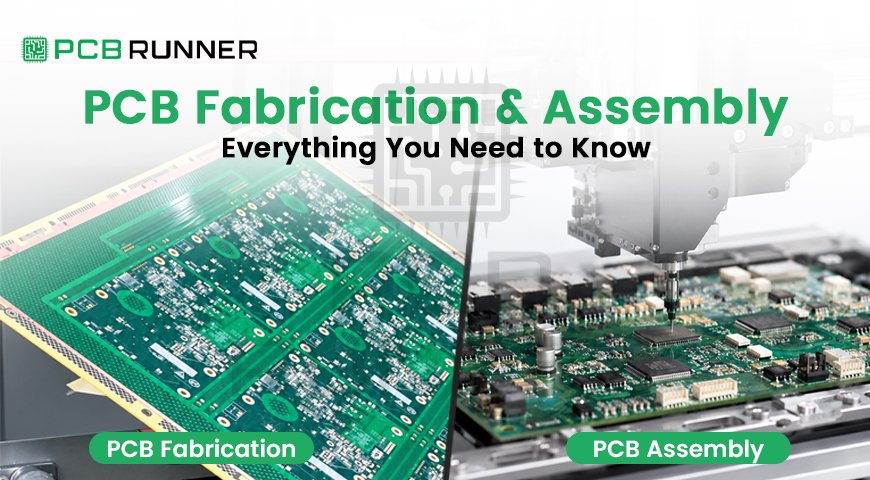
PCB fabrication and assembly is the two-stage manufacturing process that turns a circuit design into a physical, working board. Fabrication builds the bare board itself. Assembly adds the components that make it do something.
A useful way to picture it: fabrication is the construction phase, where copper layers, drilled holes, and protective coatings get built up on a substrate according to the design file. PCB fabrication ends with a bare board that has no components on it yet, just copper traces, plated holes, and a solder mask layer. The next step is PCB assembly, which involves placing resistors, capacitors, connectors, and integrated circuits on the board and soldering them in place to create a functioning circuit.
PCB Runner and most established manufacturers offer both stages under one roof, and there’s a practical reason that setup works better than splitting the job across two vendors. A board designed without assembly constraints in mind creates real problems on the production floor, things like pads sized too small for the reflow process, or trace clearances that don’t leave enough room for automated pick-and-place equipment to work reliably.
How Does the PCB Fabrication Process Work?
The PCB fabrication process follows a fixed sequence whether the board has two layers or twenty, though the tolerances tighten considerably as complexity increases.
- Design and DFM review. The fabricator checks Gerber files, drill data, and the layer stack-up against manufacturing limits. This step catches issues like trace widths under 3 to 4 mil that standard equipment can’t reliably etch, or annular rings too thin to survive drilling registration error.
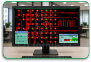
- Imaging. A photosensitive dry film gets laminated onto copper-clad substrate, then exposed to UV light through the circuit pattern, hardening the areas that will remain as copper traces.
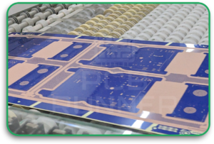
- Etching. A chemical bath, usually cupric chloride or ammoniacal etchant, dissolves the unwanted copper, leaving only the traces the design specifies.
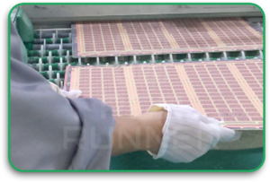
- Drilling. Mechanical drills handle standard through-holes, while laser drilling produces the microvias needed for high-density designs, sometimes down to 0.1mm in diameter.
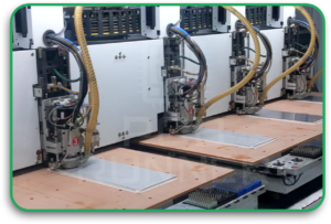
- Copper plating. Electroless and electrolytic copper deposition coat the inside of each drilled hole, creating the electrical connection between layers. Plated through-hole aspect ratios beyond 8:1 or so start pushing the limits of standard equipment.
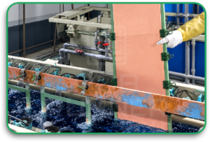
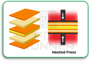
- Layer lamination. For boards with more than two layers, individual copper-clad cores get pressed together under heat and pressure, using prepreg sheets as the bonding adhesive between them. This is where a multilayer PCB actually becomes a single solid unit rather than a stack of separate pieces.
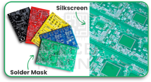
- Solder mask and silkscreen. A liquid photoimageable coating protects the copper from oxidation and solder bridging, and silkscreen printing adds reference designators and polarity marks.
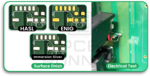
- Surface finish and electrical test. The board gets a finish, commonly HASL, ENIG, or immersion silver, and then runs through a flying probe or bed-of-nails test to confirm every net connects correctly with no shorts or opens.
Boards used in dense, compact products, the kind that rely on HDI PCB manufacturing, need tighter control at nearly every one of these steps, particularly drilling registration and layer-to-layer alignment during lamination.
What Happens During PCB Assembly?
PCB assembly is the process of placing and soldering components onto a bare board that has already passed fabrication and inspection.
Two methods dominate assembly work, and most boards use some combination of both:
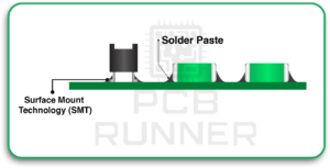
- Surface-mount technology (SMT): Components sit on pads on the board’s outer surface and get soldered through a reflow oven, typically peaking around 245°C for lead-free solder alloys. SMT supports the fine-pitch components, some with lead spacing as tight as 0.4mm, that make modern compact electronics possible.
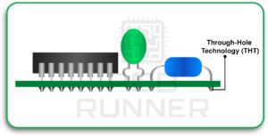
- Through-hole technology (THT): Component leads pass through drilled holes and get soldered on the opposite side, either by wave soldering or hand assembly. Connectors and larger power components still use THT because the mechanical bond holds up better under vibration and repeated stress.
A standard SMT line starts with solder paste printing through a stencil. Automated pick-and-place machines then position components on the board. Next, reflow soldering secures the components in place.
Automated optical inspection (AOI) checks for misaligned parts, tombstoning, and missing components. Boards for critical applications, such as patient monitors or flight control modules, often require additional checks.
These checks include manual visual inspection and functional testing. AOI may miss certain defects, making these extra steps important. Undetected faults can become far more expensive to fix after deployment.
Where Is PCB Fabrication and Assembly Used?
PCB fabrication and assembly touches nearly every industry that builds electronic hardware, and the requirements shift a lot depending on what the board actually has to survive.
- Medical devices: Diagnostic equipment and implantable devices need boards built to IPC Class 3 standards, where the acceptance criteria for solder joints and plating quality are the tightest in the industry.
- Aerospace and defense: Boards have to hold up under thermal cycling, vibration, and years of continuous service without a single failure, which usually rules out cheaper materials and finishes.
- Automotive: A modern vehicle carries dozens of boards, from engine control units running at high temperatures under the hood to infotainment systems that need to survive years of dashboard heat.
- Telecommunications: Network infrastructure depends on boards engineered for high-speed signal integrity, where trace impedance control matters as much as basic connectivity.
- Industrial equipment: Sensors, PLCs, and automation controllers need boards rated for continuous duty cycles, often in dusty or high-vibration environments.
- Consumer electronics: Phones and wearables push toward smaller, denser boards every product cycle, which is exactly the pressure driving demand for HDI construction.
A wearable device might lean on HDI PCB manufacturing to cram more circuitry into a few square centimeters, while an industrial control panel usually prioritizes thicker copper and mechanical durability over miniaturization.
What Should You Look for in a Manufacturing Partner?
Price matters, but it shouldn’t be the only line item you’re comparing. A few things separate a reliable supplier from one that’ll cost you more in rework down the line.
- In-house manufacturing. Suppliers who own their fabrication and assembly facilities, rather than brokering work out to third parties, catch problems earlier and hold quality more consistently across runs.
- Certifications that actually apply. ISO 9001 covers quality management, but IPC Class 2 or Class 3 qualification tells you what acceptance standard your boards will actually be held to.
- A free DFM review. A supplier who reviews your files before production starts, at no charge, will flag issues like insufficient annular ring or unrealistic aspect ratios before you’ve paid for anything.
- Honest turnaround numbers. Ask for a combined fabrication plus assembly lead time, not just the bare board timeline. Plenty of quotes only price the fabrication step and leave assembly time as a surprise later.
- Component sourcing support. A full turnkey supplier procures parts and handles sourcing for obsolete or hard-to-find components, which saves your team from chasing distributors separately.
- A named contact. When a project runs into a problem, and most complex projects eventually do, having a specific account manager who knows your job beats working through a generic support inbox.
How Much Does PCB Fabrication and Assembly Cost?
Cost swings widely from project to project, and anyone quoting a flat number without seeing your files is guessing.
- Layer count. Every additional layer means another lamination cycle and more material, which raises both price and lead time. A jump from four layers to eight isn’t a linear cost increase; it’s closer to a step change.
- Board size and order quantity. Larger production runs spread fixed setup costs across more units, while small prototype batches carry a real premium per board.
- Material selection. Standard FR-4 is the budget baseline. Specialty laminates like Rogers materials, used for RF and high-frequency boards, cost several times more per panel.
- Surface finish. HASL is the cheapest option but isn’t flat enough for fine-pitch components. ENIG costs more but gives a flatter surface and longer shelf life before assembly.
- Component complexity. Fine-pitch parts, BGAs, and dense placement all add labor and machine time to the assembly side of the quote.
- Turnaround speed. Rushing a job past standard lead time almost always carries a surcharge, since it means bumping other customers’ jobs in the production queue.
The only way to get an accurate number is to submit your actual Gerber files, bill of materials, and placement data. Anything else is a rough estimate at best.
Prototype vs. Production: What’s the Difference?
Prototype and production runs follow the same basic fabrication and assembly steps, but the goals behind each one are different enough that they need different planning.
The primary purpose of prototype PCB assembly is to identify design problems before committing to volume manufacturing. Quantities stay small, sometimes just a handful of boards, and turnaround usually runs faster since the batch is easier to slot into a production schedule. PCB prototyping at this stage is about functional verification: does the circuit work as designed, do the components fit, does the board pass basic electrical tests.
Production runs shift priorities toward repeatability and cost per unit. Once a design passes prototype testing, the process is standardized and optimized. This ensures board 1 and board 5,000 come out identical.
>Finding a routing error or footprint mismatch in a five-board prototype run costs only a few days and a modest reorder fee. However, discovering the same error after assembling 5,000 boards costs much more. It also causes significant production delays.
Conclusion
Getting a board from a design file to a working product depends on finding a partner who treats fabrication and assembly as one connected job, not two vendors passing the same project back and forth. PCB Runner reviews engineering files at no cost, manufactures boards in-house under ISO 9001 and IPC Class 2/3 certification, and supports everything from single prototypes to full production runs. If you have a design ready to move, request a free quote and get pricing back the same day for standard projects.
FAQ
Q. Is there a minimum order quantity for PCB fabrication and assembly?
Most fabricators set some threshold, but turnkey suppliers can often build small batches, including single prototype boards, without a hard minimum. Confirm directly with your supplier since this varies by shop.
Q. What files do I need to get an accurate quote?
You’ll generally need Gerber RS-274x files, a bill of materials (BOM), X&Y placement data, and any fabrication or assembly drawings that apply. Missing placement data is one of the most common reasons quotes get delayed or come back inaccurate.
Q. How long does prototype PCB assembly take compared to full production?
Prototype builds usually move faster since batch sizes are small, sometimes just a few working days. Full production runs take longer because of larger quantities and the additional quality checks that come with scaling up.
Q. Can one supplier handle both bare board fabrication and full assembly?
Yes. Many manufacturers offer turnkey service that covers fabrication, component procurement, and assembly under a single contract, which removes the coordination burden of managing two separate vendors and two separate timelines.
Q. What causes most PCB assembly failures?
Design errors that ignore manufacturing limits, like footprints that don’t match the actual component, are one of the most common causes. Poor solder joint quality and placement errors from misaligned pick-and-place equipment round out the usual list. A thorough DFM review before production starts catches most of these before they turn into an expensive rework job.



