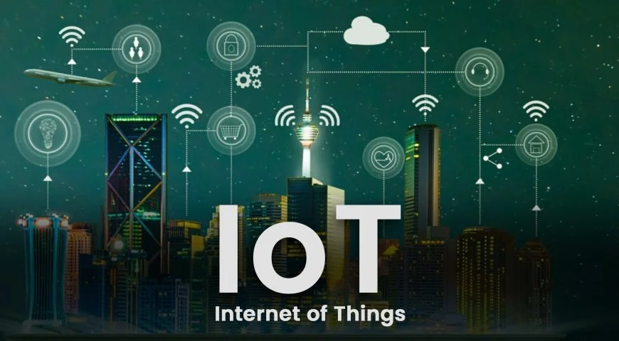
Smart devices have changed the way people interact with technology. These range from smartwatches to home automation systems, all of which rely on advanced printed circuit boards (PCBs) to work. With the expansion of the Internet of Things (IoT), the needs and importance for IoT PCBs continues to increase and is more pivotal than ever. IoT PCBs provide the backbone for numerous components to interface and guarantee that the devices communicate properly. Knowing how PCBs facilitate IoT technology is essential in the efficient design and manufacture of enhanced smart devices.
The Function of PCBs in IoT Devices
PCBs are the most essential component and vital for any device that uses the IoT ecosystem. IoT PCBs allow for accurate power distribution, data communication, and interfacing with other system components for power, data, and command signals. Rigid-flex circuits or multilayer PCBs are all available, but guidance is needed to choose the right one for a specific IoT application.
As the name suggests, IoT PCBs must be compact, versatile, dependable, and suitable for wireless communication. A myriad of IoT gadgets are designed with tiny, low-capacity PCBs integrated to enable Wi-Fi, Bluetooth, and even RFID tags. These boards must be designed with sufficient flexibility for several features while still ensuring maximum effectiveness.
Key Factors to Keep in Mind in Designing PCBs for IoT Devices
The actual design of a PCB for an IoT device requires significant attention. IoT devices usually function in compact surroundings; therefore, PCB designs must be created to enable miniaturisation. Below are some of the essential points which should be highlighted in IoT PCB designing:
- Dimension and Scope: Size is a critical design criterion for IoT PCBs, as most of them have to be placed inside a small device.
- Consumption: IoT devices are usually powered by batteries. Therefore, it is best to reduce the power consumed.
- Integration: Wireless modules like Wi-Fi, Bluetooth, or NFC need to be appropriately integrated.
- Dependability: Temperature and moisture resistance are essential because IoT devices are used in various realms.
Use of Multilayer PCBs in IoT Devices
Multilayer PCBs have long been in use for IoT applications. These types of boards are composed of conductive material in multiple layers to enable more complex circuitry within less space. These are some of the advantages when using a Multilayer IoT PCB:
- Lowered Signal Interference: Data transmission becomes more reliable the more layers of a PCB there are because the interference of other signals is greatly decreased.
- Reduced Size: More components can be packed onto the board without increasing its size.
- Increased Capability: A multilayer PCB can enable highly integrated and complex routing, which is perfect for IoT devices with multiple connections.
To meet IoT needs, manufacturers implement state-of-the-art PCB manufacturing processes, such as fine-line etching, soldering techniques, and high-density interconnects (HDI), to build multilayer boards.
The Benefits of Flex and Rigid PCBs in IoT
- Due to their advantages, flexible and Rigid PCBs are often used in IoT devices.
- Flexible PCBs are useful in the construction of wearables and medical sensors because they free up valuable space.
- Rigid PCBs, conversely, ensure device durability while acting as a support structure.
Advantages of Flex and Rigid PCBs in IoT Devices:
- Ultra lightweight: Favorable for mobile, tiny devices.
- Highly durable: Can withstand bending and shaking.
- Improved Signal Efficiency: Minimises electromagnetic interference.
Using the right type of PCB in IoT devices enhances their performance and longevity. The choice between Flex and Rigid depends on the intended application and surrounding conditions.
Challenges in PCB Production for IoT Applications
To meet the growing IoT requirements, PCB vendors must create high-grade boards that observe manufacturing constraints. Some challenges in PCB production for IoT include:
- Miniaturisation: Reducing the size and height of an IoT device requires thinner and smaller PCB conduits, which require advanced moulding techniques.
- Material Selection: The choice of substrate material is critical to heat transfer, strength, and longevity, making the right decision essential.
- Rapid Transfer Speeds: IoT PCBs need to enable quick data transfer while ensuring the signals do not weaken.
- Safeguard: IoT-related PCBs need to have restricted access so that information can be secured from unauthorised access.
To address these issues, manufacturers deploy practices such as automated optical inspection (AOI), impedance control, and thermal management strategies for enhanced quality control.
IoT and HDI PCBs
High-Density Interconnect (HDI) PCBs seamlessly accommodate the IoT ecosystem. Such PCBs enable:
- Alleviated Component Density: Squeezing more parts within a given volume.
- Increased Speed of Transmission: Better performance and minimum signal degradation.
- Reduced Power Usage: Usage of power consumption appropriate for devices operated by batteries.
Implementation of HDI PCBs increases the effectiveness and durability of IoT devices, which makes them preferable for high-end and compact devices.
Advancements in Design of IoT PCBs
New developments accompany the advancement of IoT PCB design strategies. Subsequently, there are other expected adjustments for IoT PCBs:
- Advanced 5G PCBs: With IoT systems depending on high speeds, there is a need to support PCBs for 5G technology.
- FHE: Merges standard PCBs with printed circuitry boards for versatile approaches.
- Green boards: With the rise in concern about sustainable development, there is an effort to make PCBs from eco-friendly, lead-free materials.
- Designed by AI: AI is used to optimise PCB design and increase process productivity.
How IoT PCBs Are Shaping Industries
IoT PCBs have an impact that transcends consumer electronics. Consider how they are affecting:
- Healthcare: Intelligent medical devices, remote diagnosis, and wearable health monitoring.
- Automotive: Internet of Things (IoT) in-vehicle systems, in-vehicle infotainment systems, and advanced driver assistance systems (ADAS).
- Industrial Automation: Factory automation, predictive maintenance, and smart sensors.
- Smart Homes: Home automation, connected appliances, and security systems.
Conclusion
The smart devices boom is boosting the relevance of IoT-enabled smart devices. Consequently, IoT devices rely on PCBs more than before. Choosing the appropriate Multilayer PCB, Flex and Rigid PCB, or cutting-edge IoT fabrication technology will guarantee optimal results and dependability. In the face of shifting PCB fabrication paradigms, suppliers must concentrate on IoT technology innovation, quality, and efficiencies to satisfy specifications. It is possible to construct economically viable ultra-low power smart devices with extended autonomy by knowing the PCB design for the Internet of Things.

