PCB design for assembly means laying out a board so machines can place, solder and inspect every component without defects. The most important DFA checks cover component spacing, orientation, land patterns, stencil apertures, thermal balance, fiducials, panelization and inspection access, and you should complete them before you send files to a fabricator or assembler.
Most assembly problems start in the layout, not on the line. A pad that is slightly too large, or a part tucked too close to a connector, can turn into bridging, tombstoning or a failed inspection weeks later. Fixing these at the PCB design stage costs a few minutes. Fixing them after the stencil is cut costs a re-spin.
This blog walks through ten checks you can run yourself, then explains how to verify them and what to send your assembler.
Key Takeaways
- DFA checks whether machines can place, solder and inspect your design. DFM checks whether the bare board can be fabricated. You need both.
- The ten core checks are spacing, orientation, package choice, fine-pitch land patterns, pad symmetry, stencil apertures, thermal pads and copper balance, fiducials, panel features and inspection access.
- IPC-7525 sets stencil release minimums of 1.5 for aspect ratio and 0.66 for area ratio.
- Identical pads and evenly balanced copper are the best defence against tombstoning.
- Send Gerber files, a BOM, placement data and drawings, and ask your assembler to review them before release.
What Is PCB Design for Assembly, and How Does It Differ From DFM?
Design for Assembly (DFA) is laying out a board so components can be placed, soldered and inspected reliably. Design for Manufacturing (DFM) checks whether the bare board can be fabricated. A layout can pass DFM and still fail DFA, because fabrication rules do not cover nozzle access, paste release or reflow behaviour.
In practice the two overlap, and good teams run both. DFM covers trace width, drill sizes and copper-to-edge distance. DFA covers what happens once parts arrive: placement, solder joints and inspection.
Both belong in your PCB layout design process, while parts are still easy to move.
What Are the 10 Essential DFA Checks at a Glance?
The ten checks are component spacing, orientation and polarity, package and lead spacing, fine-pitch and BGA land patterns, pad symmetry, stencil apertures, thermal pads and copper balance, fiducials, panelization features, and inspection access. Each one targets a specific assembly defect, and the table shows what to confirm.
| # | Check | What to confirm | Defect it prevents |
| 1 | Spacing and clearances | Room for nozzles, fillets, inspection and rework | Placement errors, shadowed joints |
| 2 | Orientation and polarity | Consistent direction, visible pin 1 and polarity marks | Reversed parts, slow inspection |
| 3 | Package and lead spacing | Packages your assembler can handle | Placement faults, low yield |
| 4 | Fine-pitch, BGA and QFN land patterns | Datasheet-based pads, mask dams, filled vias | Bridging, opens, hidden defects |
| 5 | Pad symmetry | Identical pads and copper connections | Tombstoning |
| 6 | Stencil apertures | Aspect ratio of 1.5+, area ratio of 0.66+ | Bridging, insufficient solder |
| 7 | Thermal pads and copper balance | Window-pane paste, even copper | Voids, warpage, weak joints |
| 8 | Fiducials | Global marks, local marks for fine-pitch parts | Misalignment |
| 9 | Panelisation and tooling holes | Rails, holes and break lines agreed with the assembler | Handling errors, damaged joints |
| 10 | Inspection access | Clear sightlines, test points, X-ray plan | Undetected defects |
What Component and Layout Checks Should You Complete First?
Start with physical placement. Check that parts have room for nozzles, soldering and rework, that polarity is consistent and visible, that package sizes suit your assembler’s equipment, and that fine-pitch land patterns match the datasheet. These checks catch the problems that stop a board from being built at all.
1. Check component spacing and clearances
Leave enough space around each part for the pick-and-place nozzle, the solder fillet and an inspection camera. Tall parts such as connectors and electrolytic capacitors need extra room, because they can shade smaller neighbours from AOI and block rework tools.
Ask your assembler for its minimum part-to-part and part-to-edge distances. Load them into your CAD design rules so violations get flagged as you work.

2. Check orientation and polarity
Place similar parts in the same direction where you can. Mark pin 1 and polarity on the silkscreen so the mark stays visible after assembly.
Consistent orientation speeds up placement and makes inspection easier. Keep silkscreen off the pads, since ink on a pad can stop solder from wetting.
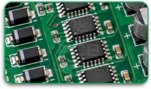
3. Check component size, package type and lead spacing
Smaller component packages require precise placement equipment and tighter process control. Before finalising the PCB layout, confirm that the assembler supports the selected component sizes, lead pitches and assembly requirements.
Where you have a choice, pick the larger size. A process that runs cleanly on 0603 parts may not suit 0402 parts.

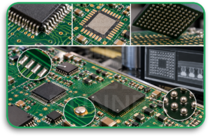
4. Check fine-pitch, BGA and QFN layouts
Build land patterns from the component datasheet and IPC-7351 recommendations. Add a solder mask dam between fine-pitch pads where the pitch allows, because it helps stop bridging.
For BGAs, check escape routing and keep any via-in-pad filled and capped so solder does not wick into the barrel. BGA joints are hidden, so plan for X-ray inspection. Add local fiducials near these parts as well (see check 8).
Which Soldering Checks Prevent Bridging, Tombstoning and Weak Joints?
Three layout areas drive most soldering defects: pad geometry, stencil apertures and thermal balance. Unequal pads cause tombstoning, oversized apertures cause bridging, and starved apertures or copper that drains heat cause weak or incomplete joints. Check all three before you release files.
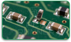
5. Check pad symmetry to avoid tombstoning
Tombstoning happens when one end of a small chip part wets before the other, and surface tension pulls the part upright. It mostly affects light parts such as 0402 and 0201 packages.
Keep both pads identical in size, shape and copper connection. Avoid joining one pad to a large plane while the other connects to a thin trace, because the plane acts as a heat sink during reflow. If a pad must join a plane, use thermal relief so both pads heat at the same rate.
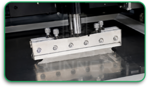
6. Check solder paste apertures and pad design
IPC-7525 provides stencil design guidance, including commonly used minimum aspect and area ratios of 1.5 and 0.66, respectively. These ratios help assess potential solder paste release, although actual printing performance also depends on aperture geometry, stencil quality and solder paste properties.
Work out both for your smallest pads. A 0.25 mm by 0.6 mm opening in a 0.12 mm stencil gives an area ratio of about 0.74, which passes. A low ratio leaves paste stuck in the aperture and the joint starved. An aperture too large for the pad pitch pushes paste sideways, and it bridges.
7. Check thermal pads and copper balance
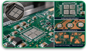
A large exposed pad, like the one under a QFN, can trap flux gas and form voids if you print one solid block of paste. A window-pane pattern covering roughly 50 to 80 percent of the pad lets the gas escape. Check the component datasheet for its exact recommendation, and cover or fill thermal vias so solder does not wick away.
Copper balance matters too. Uneven copper across layers can warp the board, and large copper areas beside small pads pull heat away during reflow. Spread copper evenly and use thermal reliefs on pads that connect to planes.
How Should You Prepare the Board for Automated Assembly and Inspection?
Automated lines need reference points, a stable panel and clear sightlines. Add fiducials so machines can align the board, design panel rails and tooling holes to your assembler’s rules, and leave room for AOI, X-ray and test probes. Skipping these features slows setup and reduces inspection coverage.
8. Check fiducials
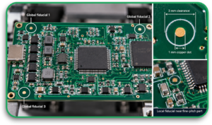
Fiducials are small copper marks that machines use to find the board’s position. A common specification is a 1 mm copper dot with a 3 mm clear area and no other pads, holes or traces inside it.
Use at least two global fiducials. Three, spread as far apart as possible, help the machine correct for stretch or twist. Add local fiducials near large or fine-pitch parts, and keep the size consistent across the board.
9. Check panelization and tooling holes
Small boards usually run in panels, so design the panel together with your assembler. Agree on rail width, tooling hole positions, the breakaway method (V-score or routed tabs) and where the global fiducials sit on the rails.
Keep components away from break lines so depaneling does not stress solder joints. Requirements differ between lines, so ask for the assembler’s panel specification before you finish the layout.

10. Check access for AOI, X-ray and test
AOI is effective for inspecting visible solder joints but cannot directly examine hidden connections beneath BGAs and exposed QFN pads. X-ray inspection can help identify internal defects such as solder bridging and voiding, while electrical testing provides additional verification of circuit performance.
- tall parts placed right beside small ones
- fine-pitch parts hidden under shields or fixed connectors
- silkscreen covering pads
- no accessible test points
PCB Runner offers AOI, X-ray and in-circuit tests, so leave space for whichever your board needs.
How Do You Verify Your Layout Meets DFA Requirements Before Production?
Run your CAD design rule check with your assembler’s limits loaded, then review the 3D model, assembly drawing and paste layer against the ten checks. Finish with a manufacturer review of your actual files, because the assembler knows its own line’s limits.
A simple verification routine looks like this:
- Load your assembler’s spacing, silkscreen and mask rules into the design rule check.
- Open the 3D view and look for height clashes and blocked connector access.
- Calculate aspect and area ratios for your smallest pads.
- Review the paste layer, especially thermal pads and fine-pitch parts.
- Ask for a pre-production review before you place the order.
What Files Should You Send, and Can a Manufacturer Check Your Design?
Send Gerber RS-274x files, a bill of materials, X and Y placement data, and fabrication and assembly drawings. A manufacturer can review these files before production. PCB Runner protocols are to review all CAM files from design for assembly (DFA) and design for manufacturing (DFM) perspective before starting manufacturing and assembly.
Your BOM should list quantity, reference designator, manufacturer name and manufacturer part number. If you are working with a UK or European assembler, also state the IPC class you need and whether the build must be lead-free for RoHS. Clear notes up front, save back-and-forth emails.
For turnkey builds, PCB Runner’s PCB assembly service covers SMT and through-hole work from one supplier, with no minimum order quantity.
FAQs
What is the difference between DFA and DFM in PCB design?
DFM asks whether the bare board can be fabricated, using rules for trace width, drill size and copper spacing. DFA asks whether components can be placed, soldered and inspected. Both reviews are needed, because passing one does not guarantee the other.
When should I start DFA checks?
Start during component placement, before routing is final. Spacing, orientation and package choices are easy to change at that stage. By the time the layout is complete, the same changes can mean re-routing large parts of the board.
What causes solder bridging on a PCB?
Bridging usually comes from too much paste, apertures that are too large for the pad pitch, pads placed too close together, or missing solder mask dams between fine-pitch pads. Checking aperture size against pad pitch and adding mask dams reduces the risk.
Do I need fiducials on every PCB?
Any board built on an automated SMT line should have them. Two global fiducials are the minimum, and three help with distortion. Small boards may run with global marks only, but confirm with your assembler.
Why do BGAs need X-ray inspection?
BGA solder balls sit under the package, so cameras cannot see them. X-ray shows bridging, voids and missing balls beneath the part, which is why you should plan for it during layout.
Conclusion
The ten checks above cover the layout mistakes that most often cause assembly defects. Run them while parts are still easy to move, load your assembler’s rules into the design checker, and send complete files with clear notes.
If you want a second opinion before you commit to a build, send your files to PCB Runner for review.