Ultra-Thin vs. High Layer Count Rigid PCBs: Key Differences
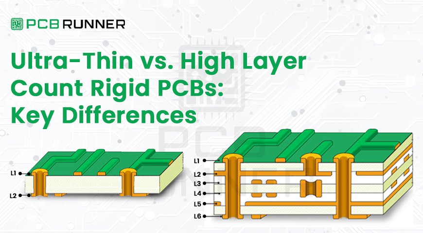
Objective Explain the difference between an ultra-thin rigid PCB and a high-layer-count rigid PCB in plain language. You’ll see what […]
Objective Explain the difference between an ultra-thin rigid PCB and a high-layer-count rigid PCB in plain language. You’ll see what […]
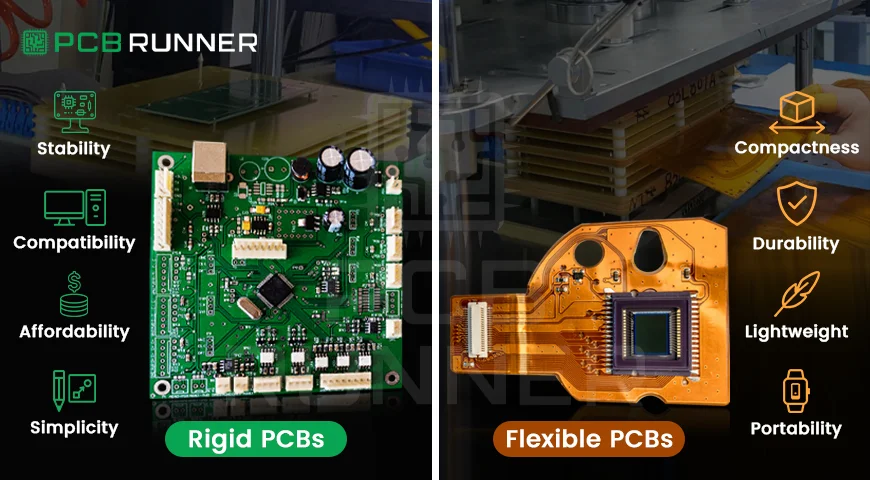
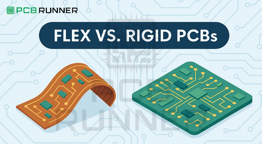
In the world of PCBs, we frequently encounter two distinct types: rigid PCBs and flexible circuits. While both serve the
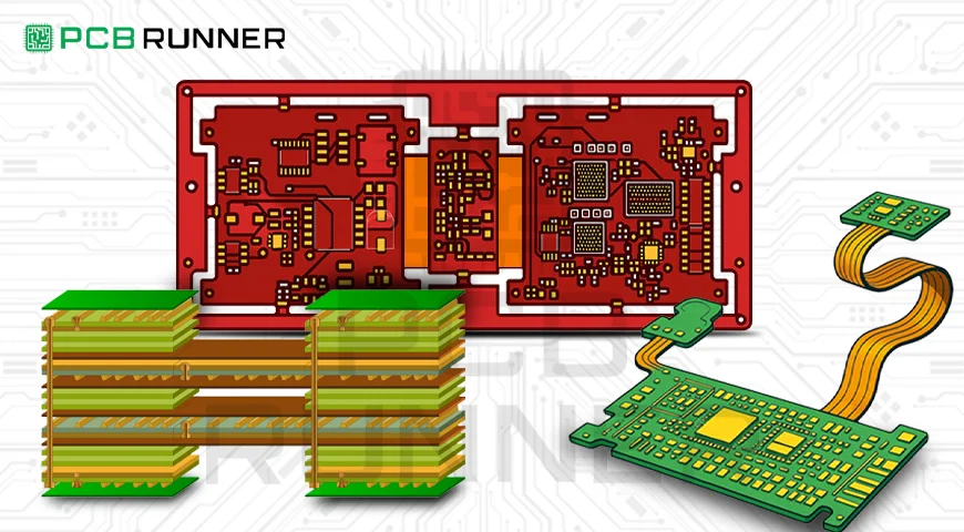
Rigid-flex PCBs are changing how we design electronic devices. By combining flexible and rigid sections, they allow for compact, durable,
Electronics are getting smaller, smarter, and more powerful. Whether it’s your phone, smartwatch, or car dashboard, everything needs compact and
When most people think about electronics, they picture flat, rigid circuit boards inside phones, TVs, and computers. But did you
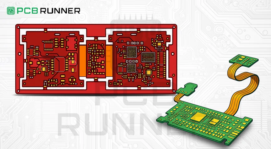
With the increase in the usage of modern day electronic devices, the need for complex, compact rigid-flex PCBs has gone
Printed Circuit Boards (PCBs) are critical in every electronic gadget as they ensure the mechanical and electrical interconnections between different

To keep up with the demand for modern electronics, industries are pivoting towards Rigid-Flex PCBs, which are a step in
Why IoT Devices Rely on Rigid HDI PCB Substrates The Internet of Things (IoT) is improving at a rapid pace,
Over the past few years, printed circuit board technology has advanced dramatically. It demands goods that are both faster and

Fill out our comprehensive online PCB & Assembly specification form and receive instant pricing via email.

Have any advanced capability PCB design? Upload your files for our review and get a personalized quote from our Sales Engineer Executive via email.