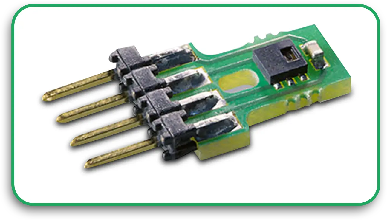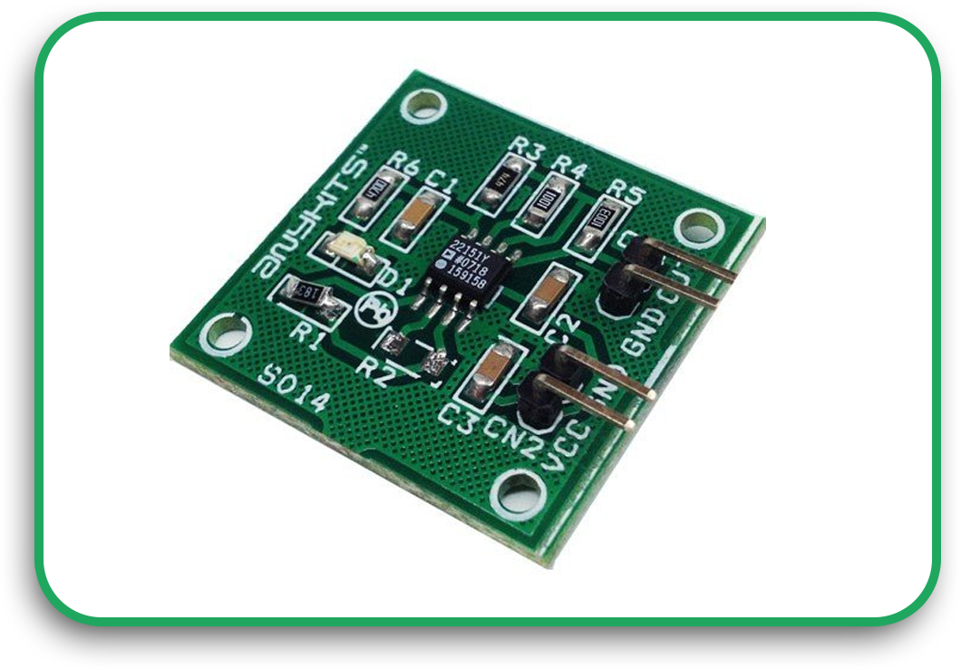
When working with any printed circuit board (PCB), one important detail you should never overlook is the solder paste mask. While it may seem like a thin layer of colour on the board, the paste mask plays a key role in how well your board works. It impacts everything from the board’s strength to how it performs under stress.
In this blog, you will learn how solder paste masks work, what materials are used, and why they matter so much. You will also see how these masks support high-density interconnect designs and improve your PCB board assembly process.
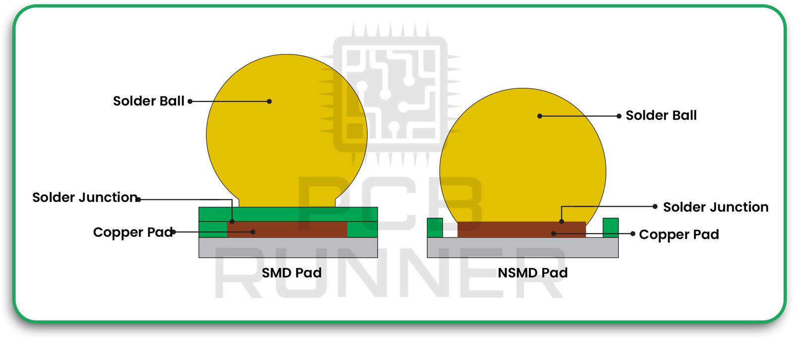
What Is a Solder Paste Mask?
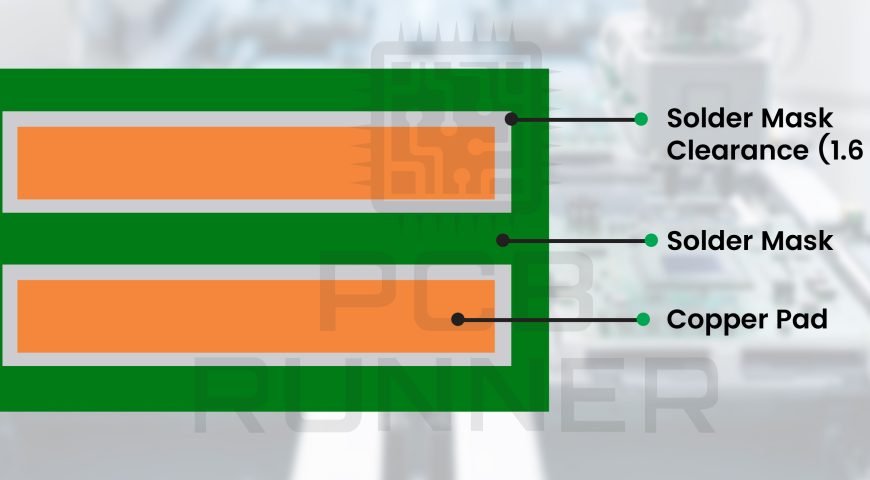
A solder paste mask, often simply called a solder mask, is a protective layer placed on a PCB. This layer covers the areas where you do not want the solder to stick. It also leaves openings where you want the solder to go during the assembly process.
The most common type of solder mask is made using epoxy or liquid photoimageable (LPI) solder mask material. These materials are chosen for their ability to stick well to the board and for how well they resist heat and moisture.
Why Use a Solder Paste Mask?
You might wonder why you even need this layer. Here are a few reasons:
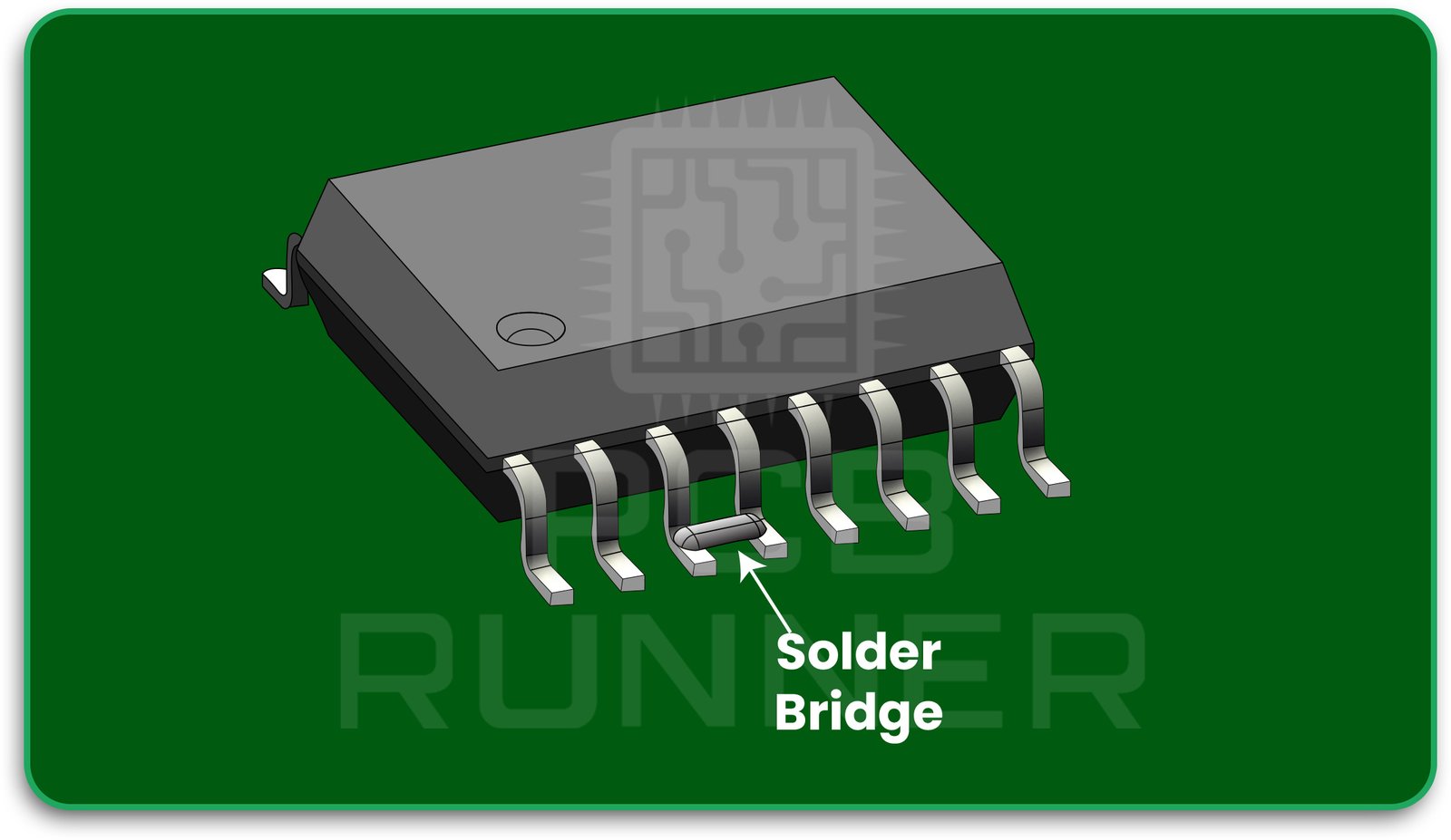
- Prevents solder bridging: It keeps solder from connecting parts that should not be connected.
- Improves board durability: It protects the board from moisture, dust, and other damage.
- Helps with PCB solder mask alignment: It ensures solder goes only where it should during reflow.
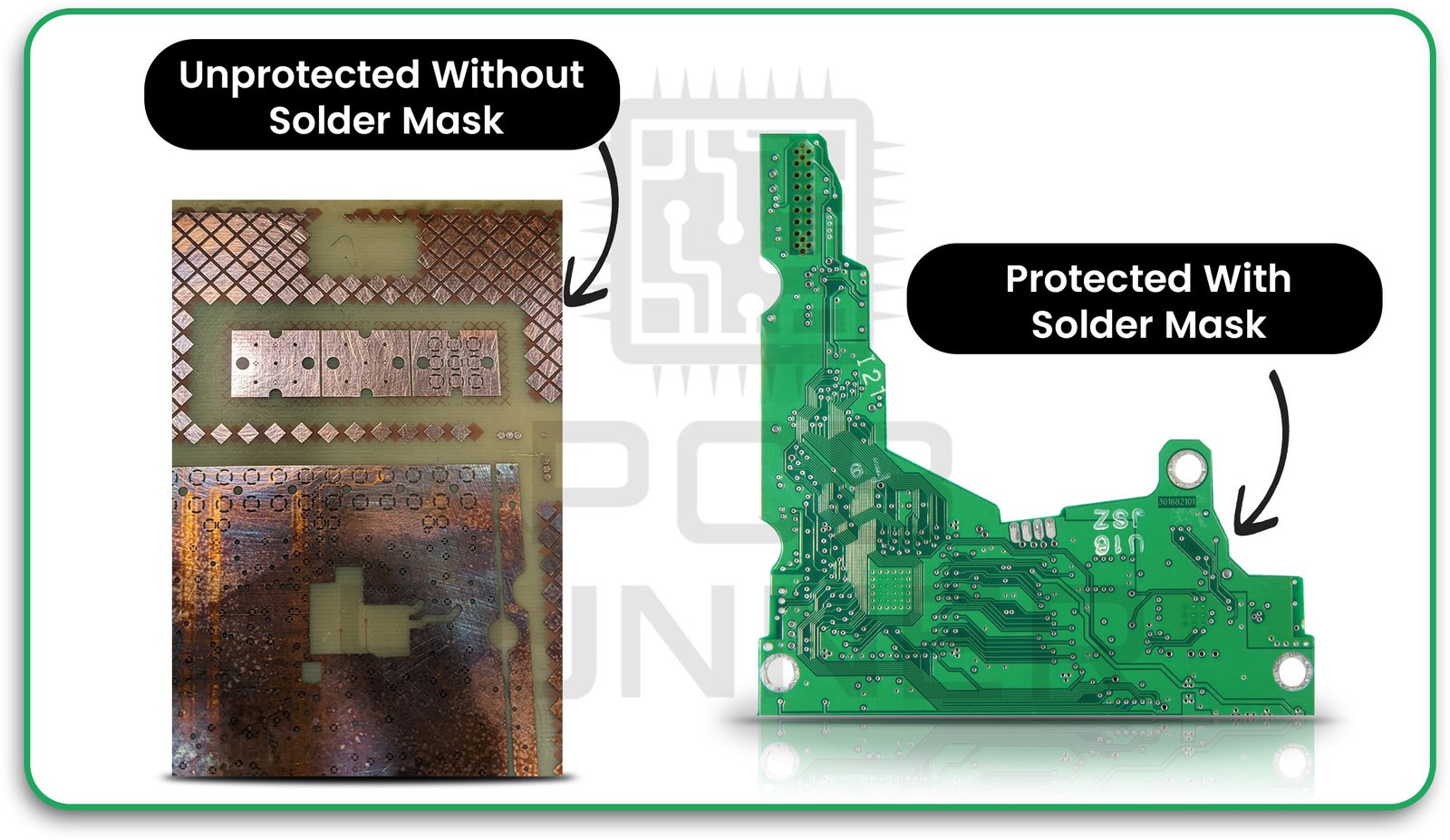
Without a solder mask, your PCB can short out more easily or wear down faster. So, even though it is a small part of the board, it has a significant impact.
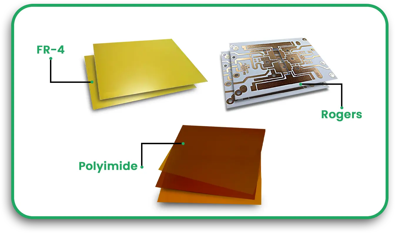
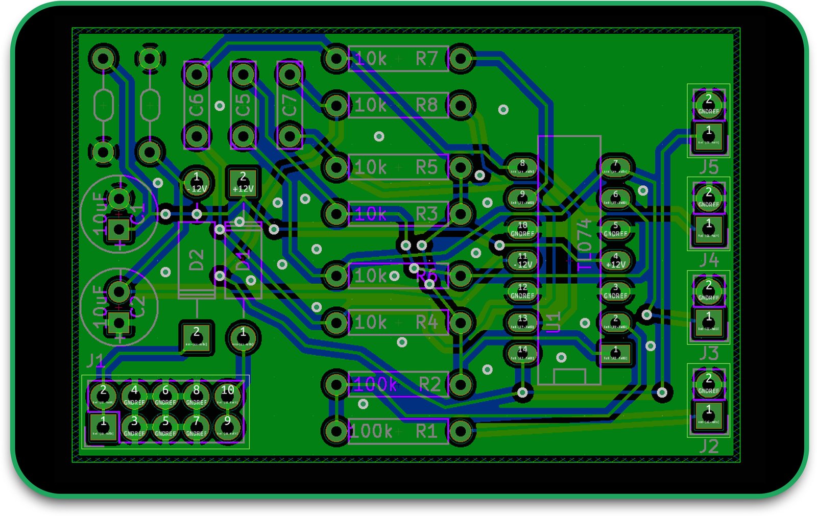
Types of Solder Mask Materials
There are different types of solder mask materials, and the right one depends on how your board will be used:
- Epoxy liquid: This is a lower-cost option. It is applied with a screen printing method. It works well for simple PCBs.
- LPI (Liquid Photoimageable): This is the most common option for modern circuit boards. It gives better accuracy, especially for high-density interconnect boards.
- Dry film: This is used when the board design needs very tight spacing and high resolution.
When you choose the best solder mask material for your project, you help improve the life and performance of your circuit board.
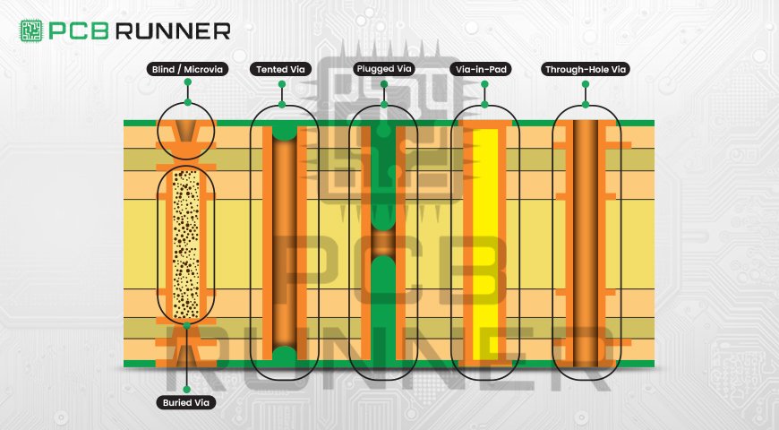
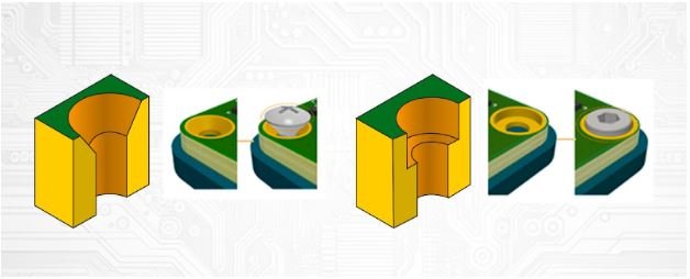
Paste Mask in PCB: What Does It Do?
The paste mask is closely related to the solder mask, but they are not the same thing. The paste mask defines where solder paste should be applied. This happens before the board is placed in a reflow oven.
The paste mask ensures that paste is applied only to pad areas, not on traces or open board space. This step is crucial when your design includes a high number of small parts, like in a high-density interconnect board.
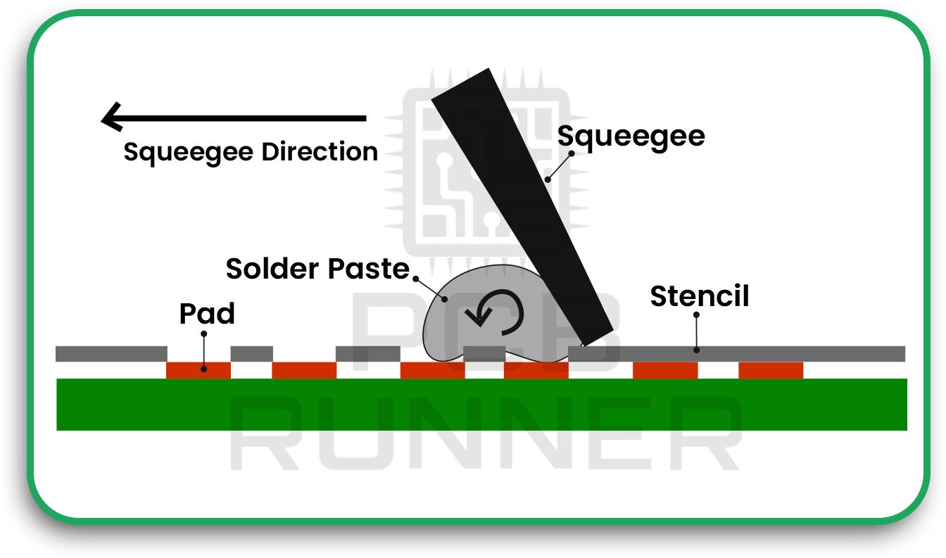
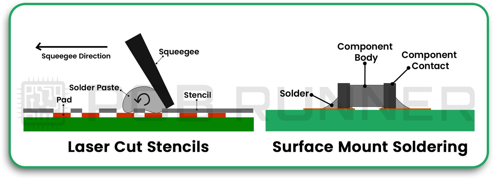
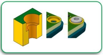
How the Solder Mask Helps in PCB Board Assembly
During PCB board assembly, accurate paste placement is critical. The solder mask keeps paste from flowing into unwanted areas. This protects nearby parts from getting too much heat or unwanted solder during reflow.
In boards with small components or tight spacing, like those made by advanced pcb circuit board manufacturers, this becomes even more important. Paste mask and solder mask work together to make sure assembly is smooth and your board ends up strong.
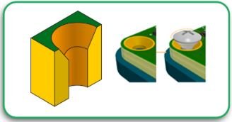
Board Paste Flow and Control
One key benefit of having a good solder paste mask setup is better control of paste flow. When the paste goes only where it should, you get stronger joints, fewer solder balls, and less chance of failure.
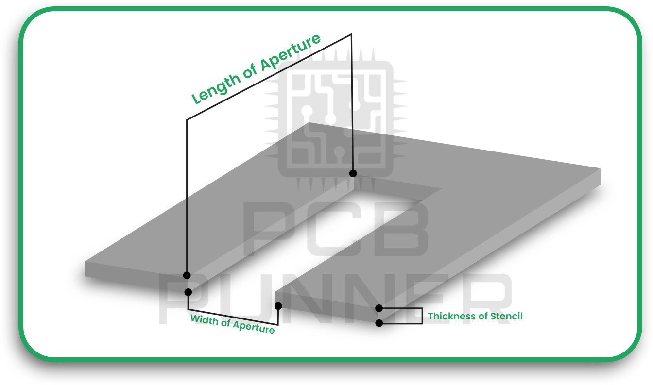
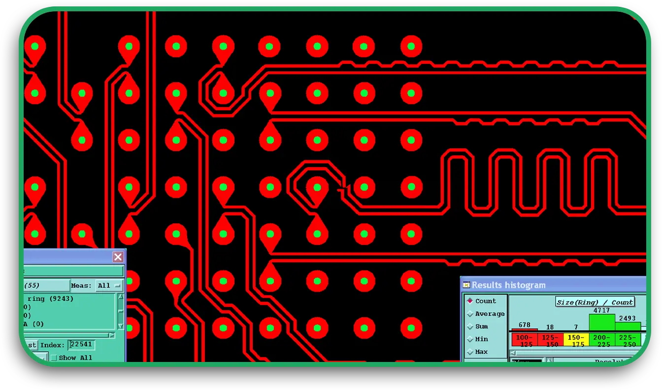
For example, on a high-density interconnect board, solder mask openings must be exact. Even small mistakes in the opening size or placement can lead to solder bridges or weak connections. Using the right paste mask in PCB design keeps those problems from happening.
PCB Solder Mask Colors and What They Mean
While green is the most common colour, solder masks also come in red, blue, white, black, and other shades. These colours are mostly for looks or specific lighting requirements during testing and inspection.
However, you should know that some colours make visual inspection easier. For example, green shows contrast better for human eyes, which can be helpful during manual checking.
Some PCB manufacturers offer custom solder mask colours to fit brand or functional needs.
Solder Mask Design Tips
Here are a few helpful tips when working on your board’s solder mask:
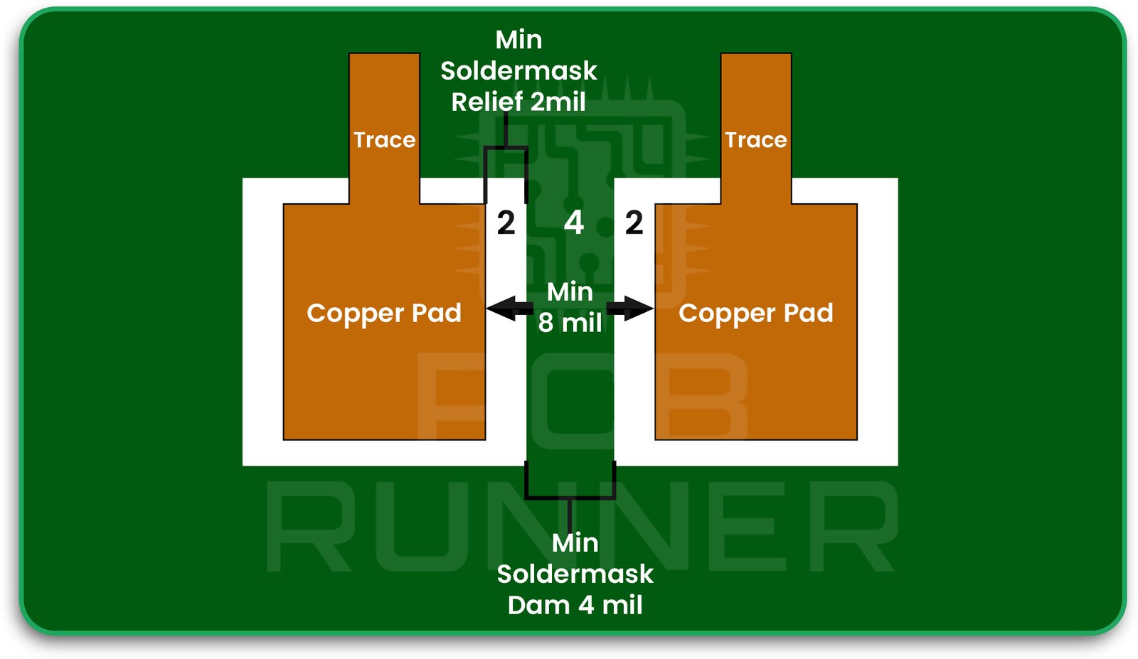
- Match it with pad sizes: Keep the mask opening slightly larger than the pad to allow for placement tolerance.
- Use solder mask relief: This keeps the mask from peeling or lifting over time.
- Review high-density zones carefully: Pay close attention to BGA and fine-pitch parts.
Making the right design choices for solder masks saves you from costly fixes later in the process.
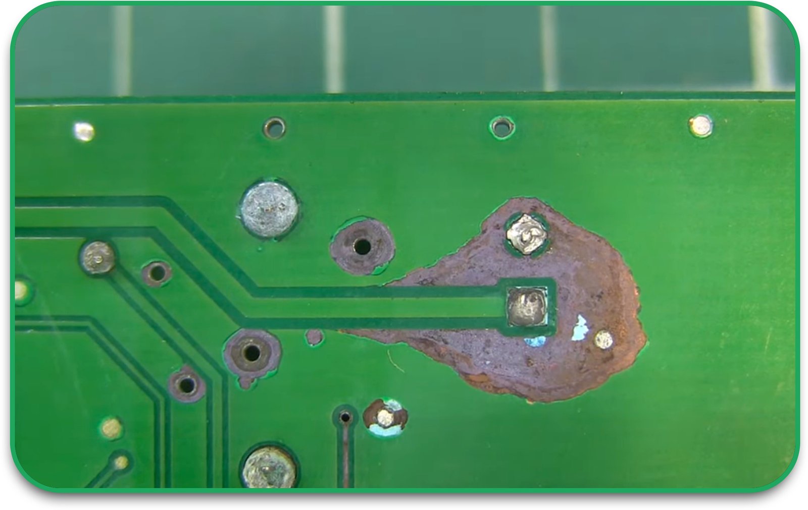
What Happens If You Skip the Solder Mask?
You might think of skipping the solder mask if your board has very few parts. But doing so can lead to:
- Short circuits
- Moisture damage
- Poor solder quality
- Decreased product lifespan
Even simple boards benefit from this extra protection. Most pc board manufacturers will include it as part of standard PCB fabrication.
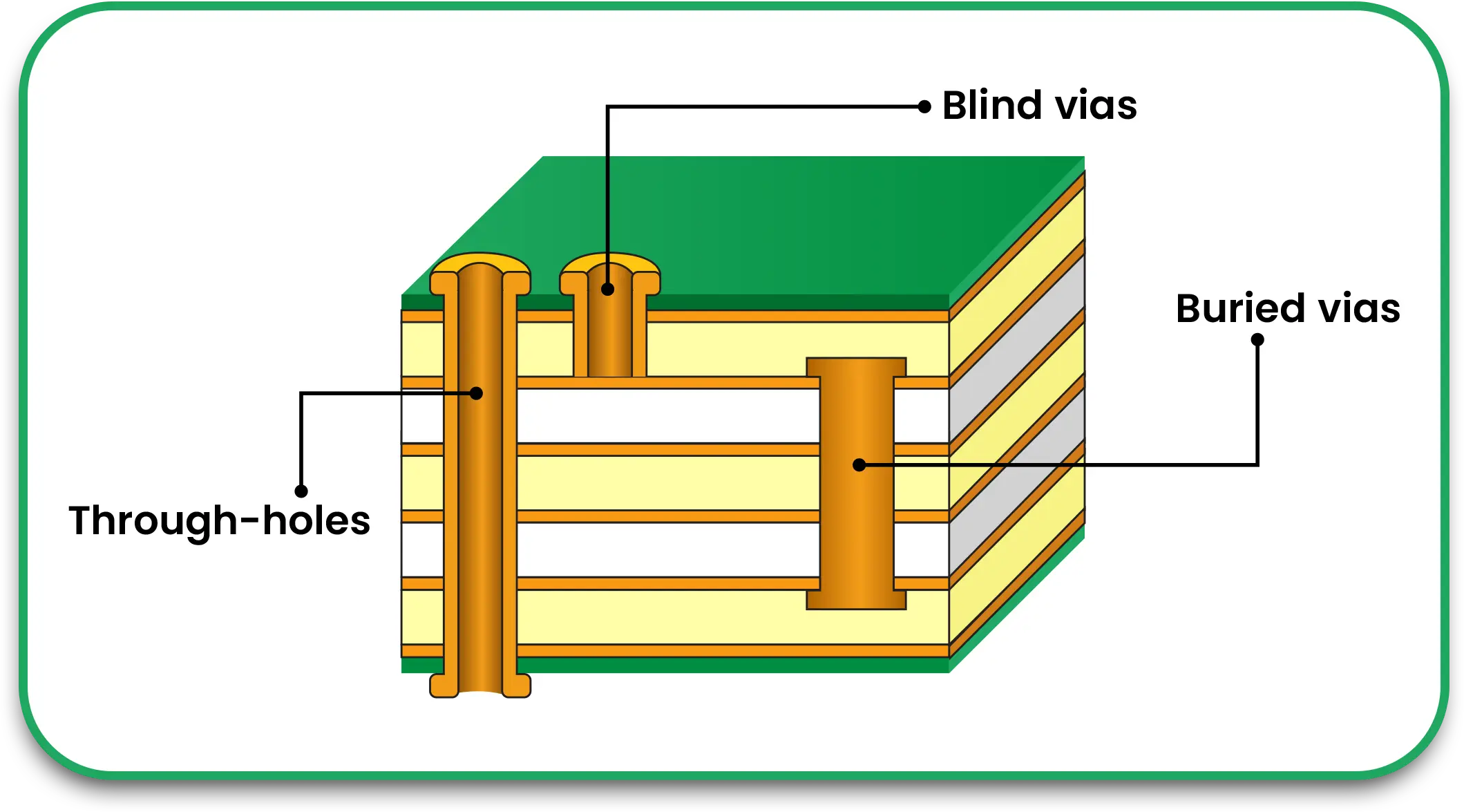
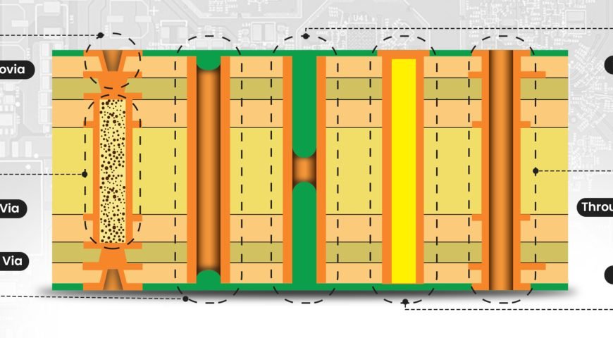
Role in High-Density Interconnect Boards
When it comes to high-density interconnect PCBs, solder mask design becomes critical. These boards pack more connections in less space. That means paste and solder have very little room for error.
The solder mask helps guide the paste to the correct locations. This prevents bridging or weak joints, even when using microvias and tiny SMD parts.
So, if you are working with a high-density interconnect board, pay close attention to your solder mask layer. It could make or break your board’s reliability.
Trust PCB Runner for Quality PCB Board Assembly
If you want a PCB that works the first time and lasts long, do not ignore your solder paste mask. It protects your board, controls solder flow, and ensures clean assembly.
Whether you need simple boards or complex high-density interconnect solutions, getting the solder mask right is key.
At PCB Runner, we focus on quality from start to finish. Our team pays close attention to every detail, including solder mask material, board paste control, and paste mask alignment. As experienced PCB circuit board manufacturers, we ensure your PCB board assembly meets the highest standards.
Contact PCB Runner today to learn how we can help with your next project. Your board’s performance starts with smart choices in every layer.