Tg in core

Understanding the Importance of Tg in Core and Pre-preg for PCB Manufacturing

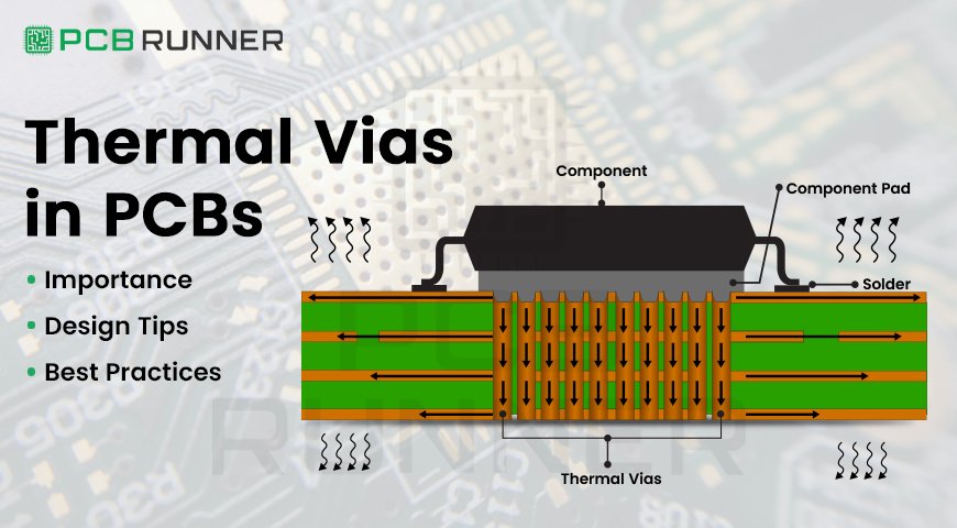
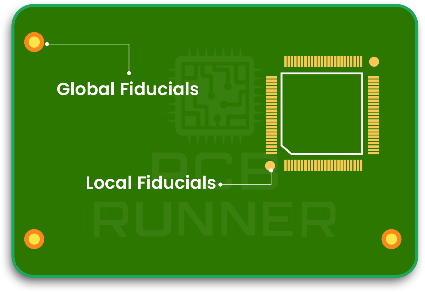
Think about how your phone, laptop, or car’s control system works. Each one depends on a printed circuit board (PCB) inside it. These boards keep electronic components connected and working correctly. But one hidden factor makes all the difference in how durable a PCB is, the material’s Tg value.

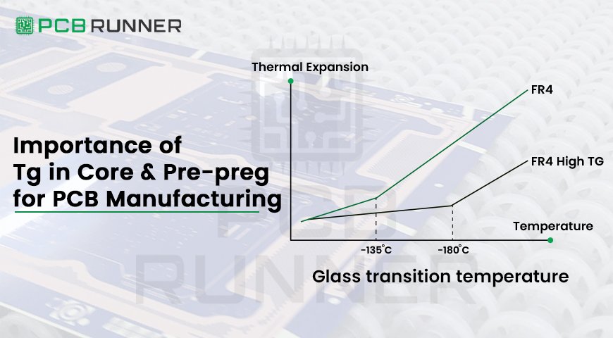
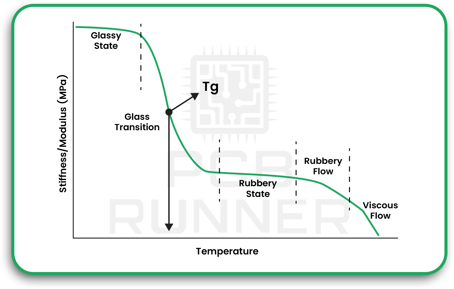
The term Tg refers to the glass transition temperature in PCB manufacturing. Tg is the temperature where the PCB’s resin system changes from rigid to soft ,  not a heat-resistance limit, but a key indicator of thermal stability. Understanding Tg helps engineers design more reliable circuit boards. PCB Runner highlights the importance of picking the right Tg value for both core and pre-preg materials so every board can handle real-world heat and stress.

At PCB Runner, a leader in PCB production in the UK, we emphasize selecting the right Tg for both core and pre-preg materials to ensure superior performance, longevity, and manufacturing precision.

What Is Tg and Why Does It Matter in PCBs

Definition of Tg

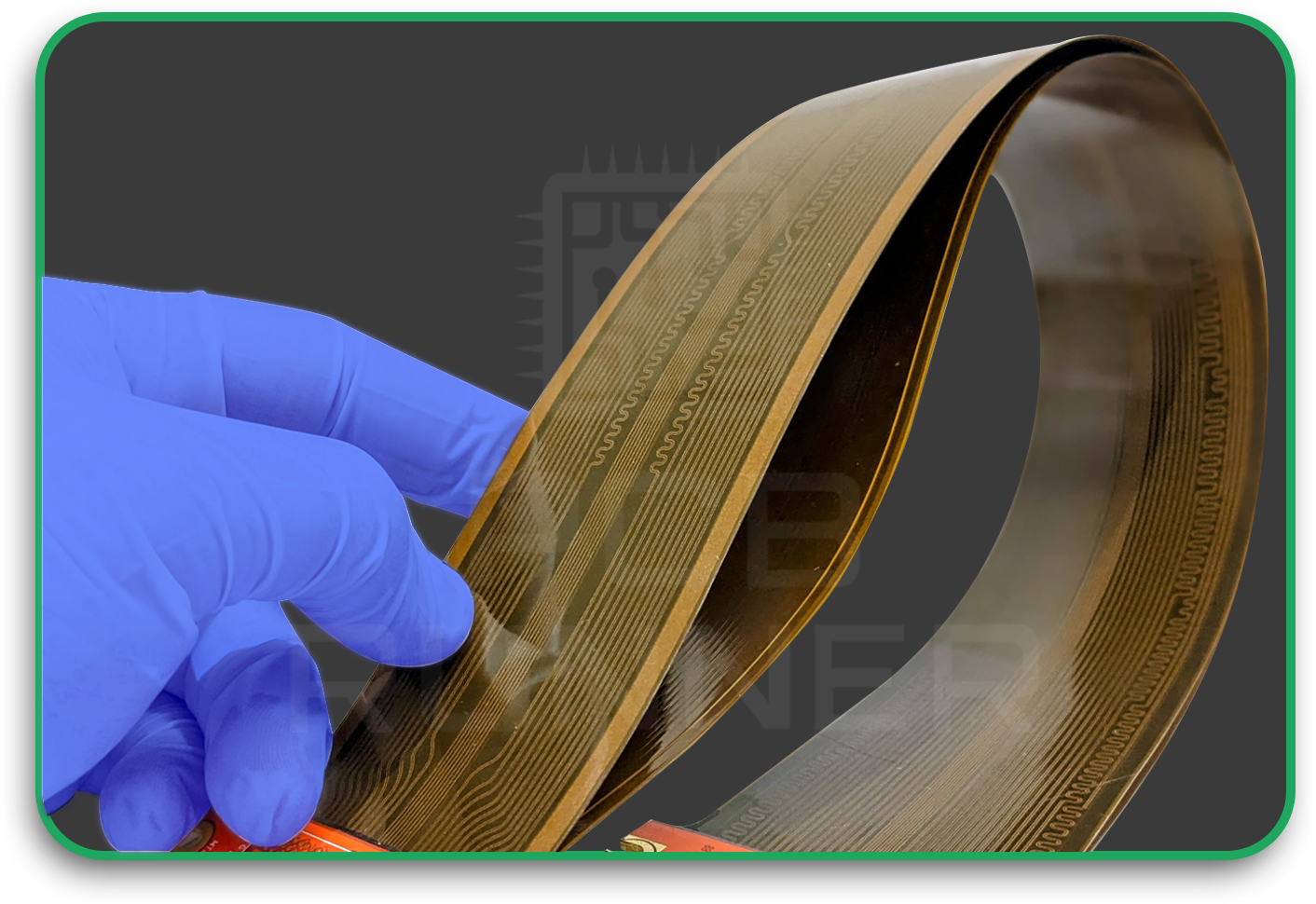
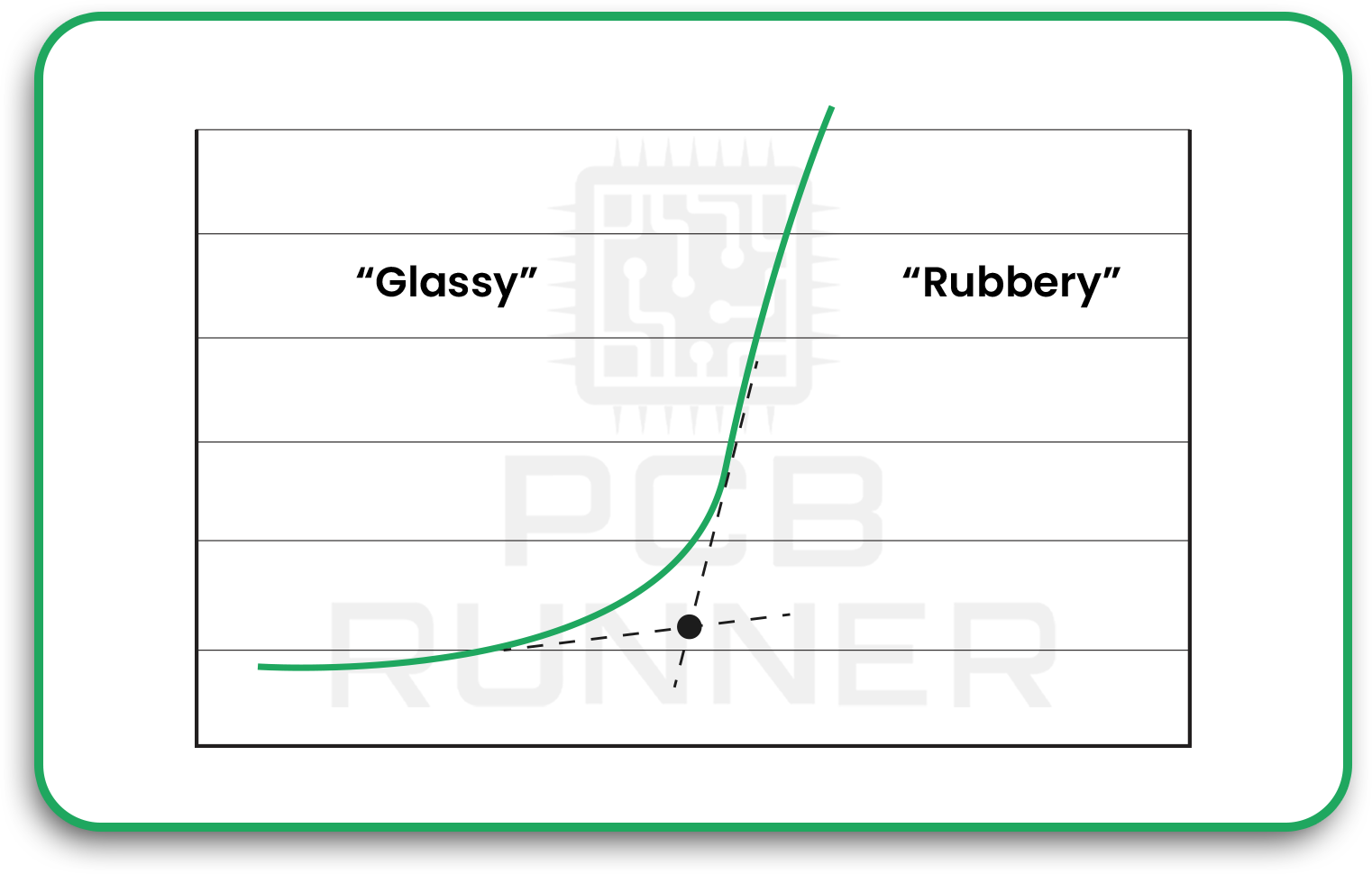
Tg is the temperature at which the PCB’s resin system ,  not the glass fibre itself ,  changes from a rigid to a rubbery state. Below Tg, your board stays firm and stable. Once the heat rises above that level, the material becomes flexible and loses its shape.

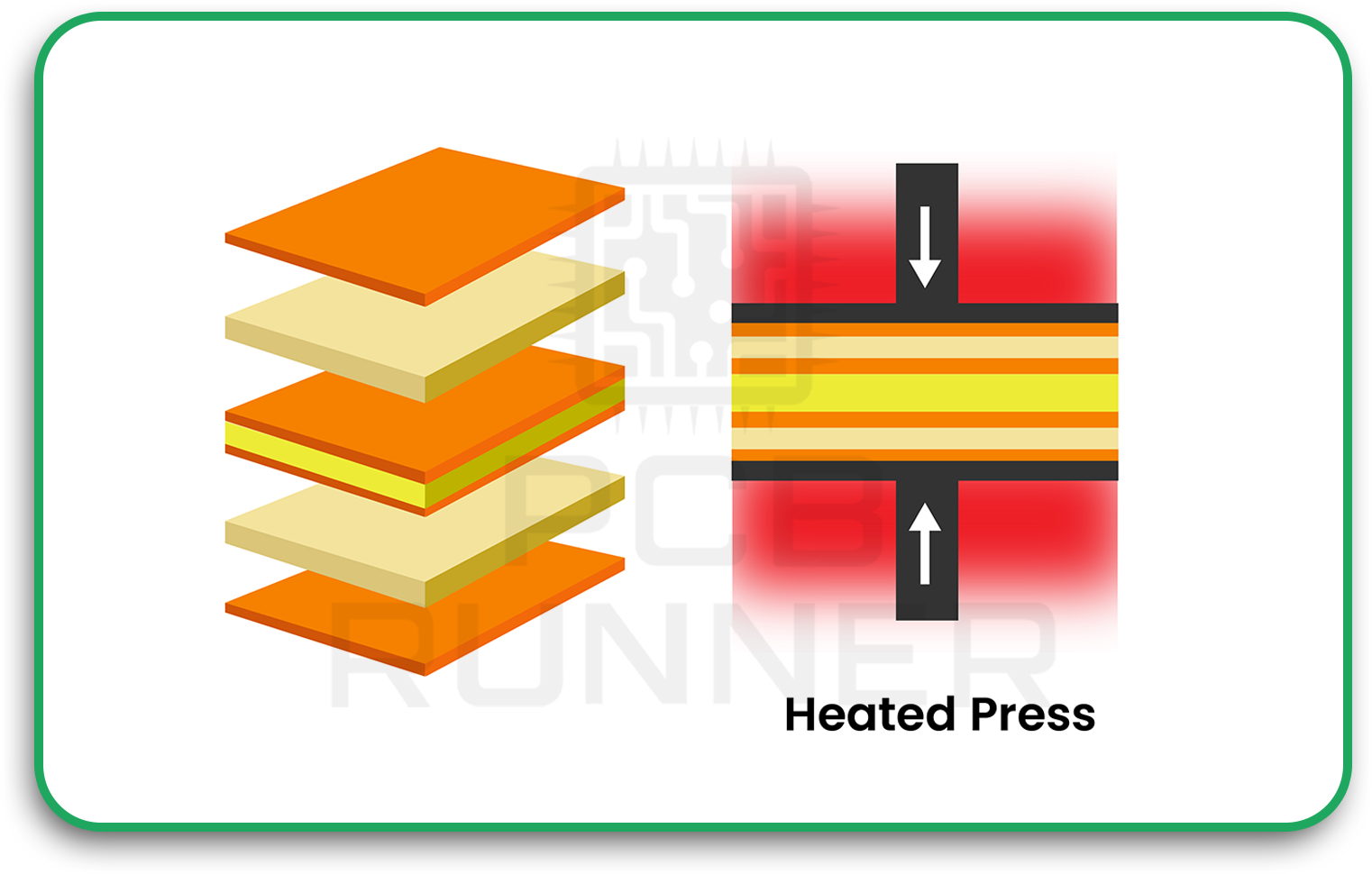
During PCB manufacturing, the board faces high heat when components are soldered or when the layers are laminated together. So, selecting a proper Tg value helps the board stay stable and strong throughout the entire process.

Definition of Tg

Relationship Between Tg, Heat, and Reliability

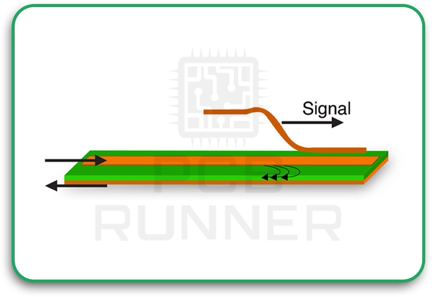
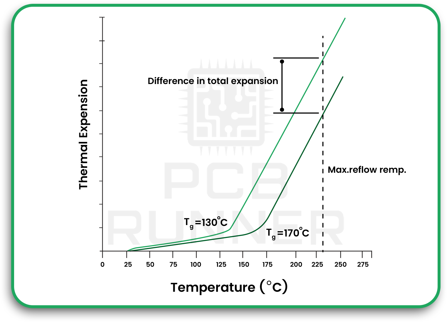
When a board heats during assembly or operation, it expands; when cooled, it contracts. If Tg is too low, it cannot handle this change. Cracks, warping, and broken connections can follow. Boards with a higher Tg can survive repeated heating cycles, keeping your circuit reliable for years.

Relationship Between Tg, Heat, and Reliability

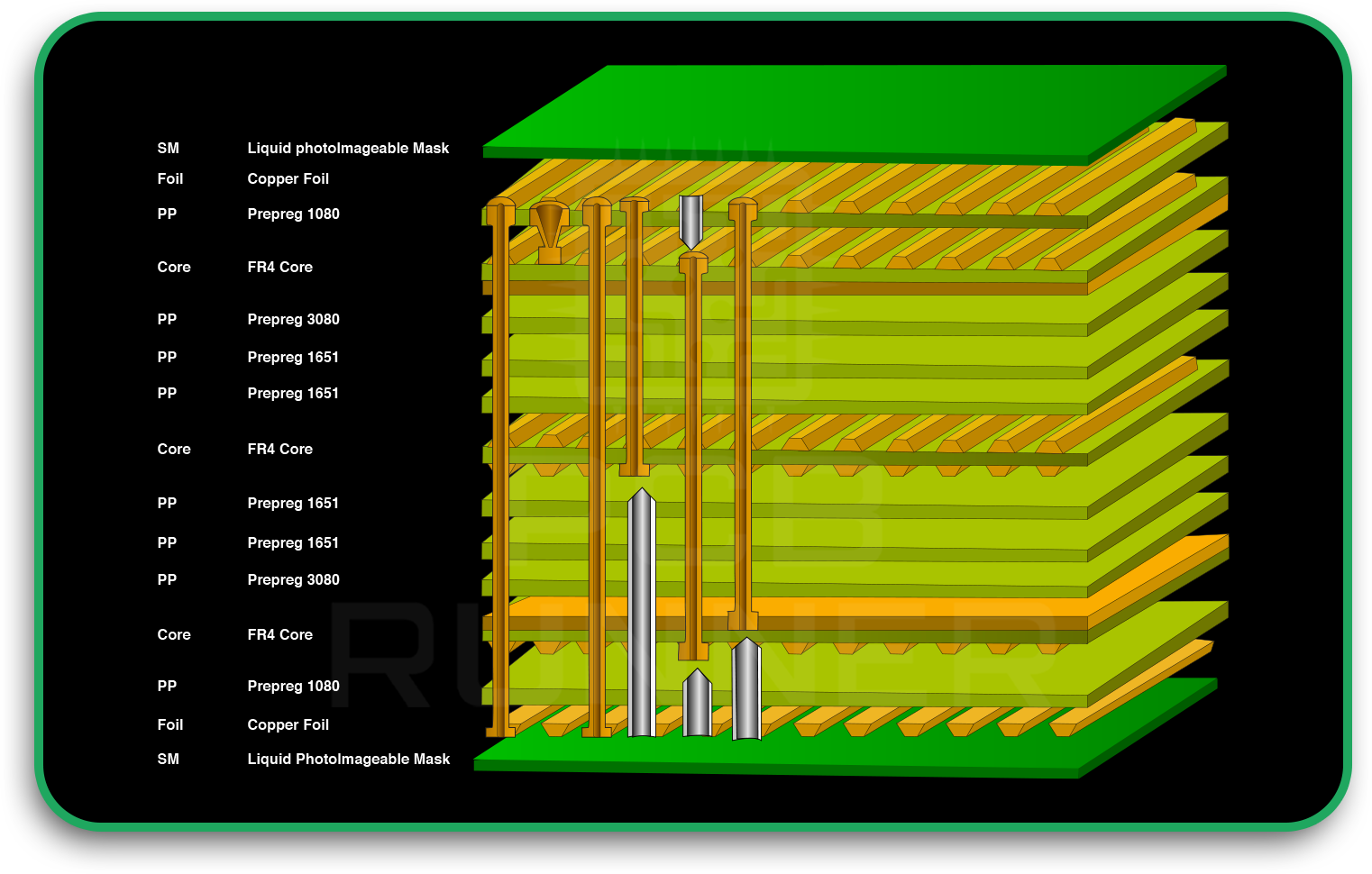
Core and Pre-preg Materials – The Building Blocks of a PCB

What Are Core and Pre-preg Layers

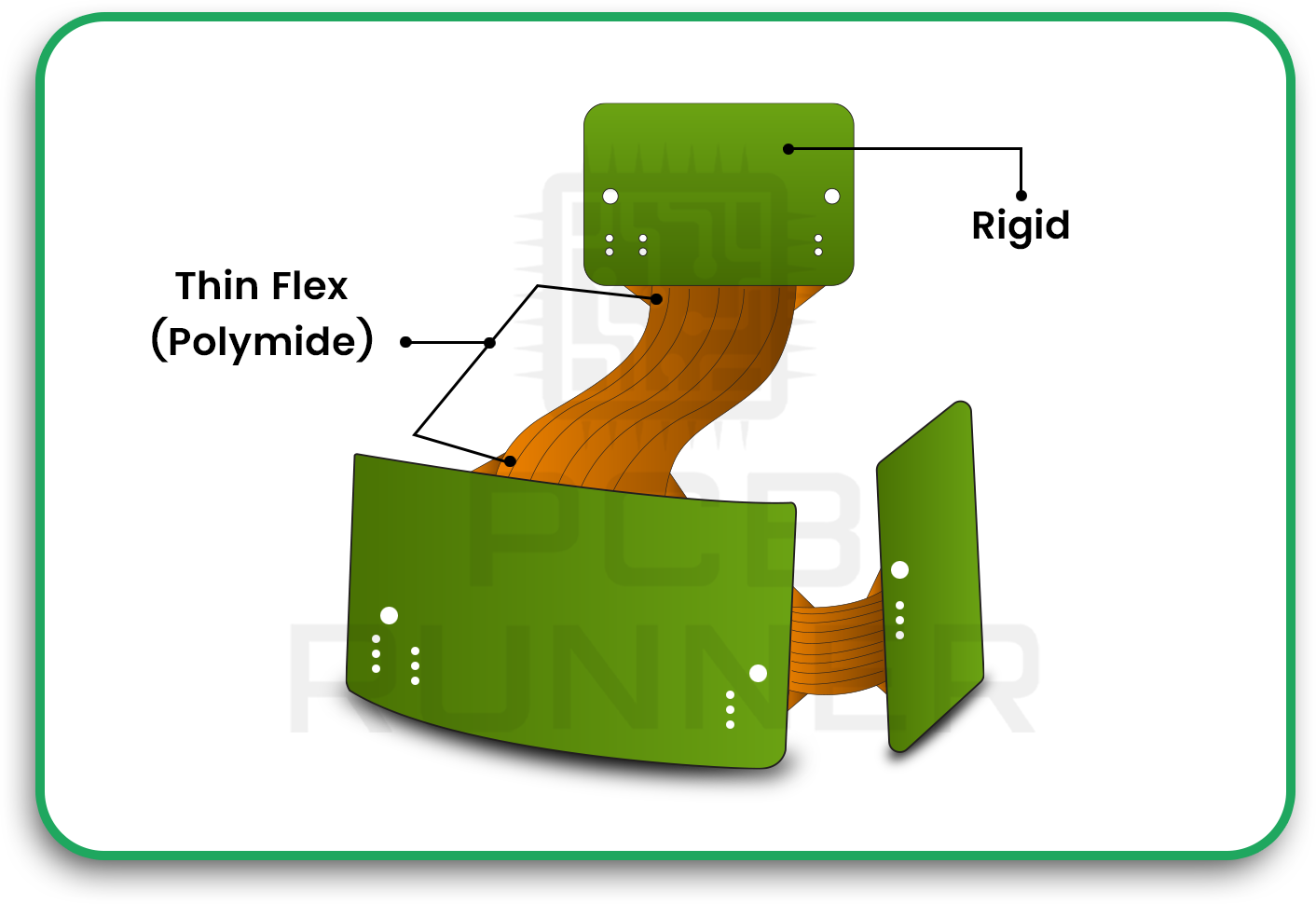
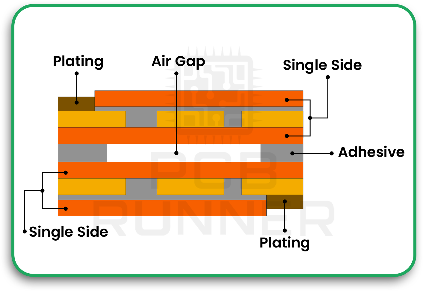
A PCB is made of multiple layers joined together. The core is a stiff sheet made of fibreglass and resin. The pre-preg is a layer of fibreglass cloth coated with partially cured resin. When both are heated, they bond to form one strong, solid unit.

These layers decide how thick your PCB will be and how well it can handle heat and mechanical stress.

What Are Core and Pre-preg Layers

How Tg  Affects Core and Pre-preg Performance

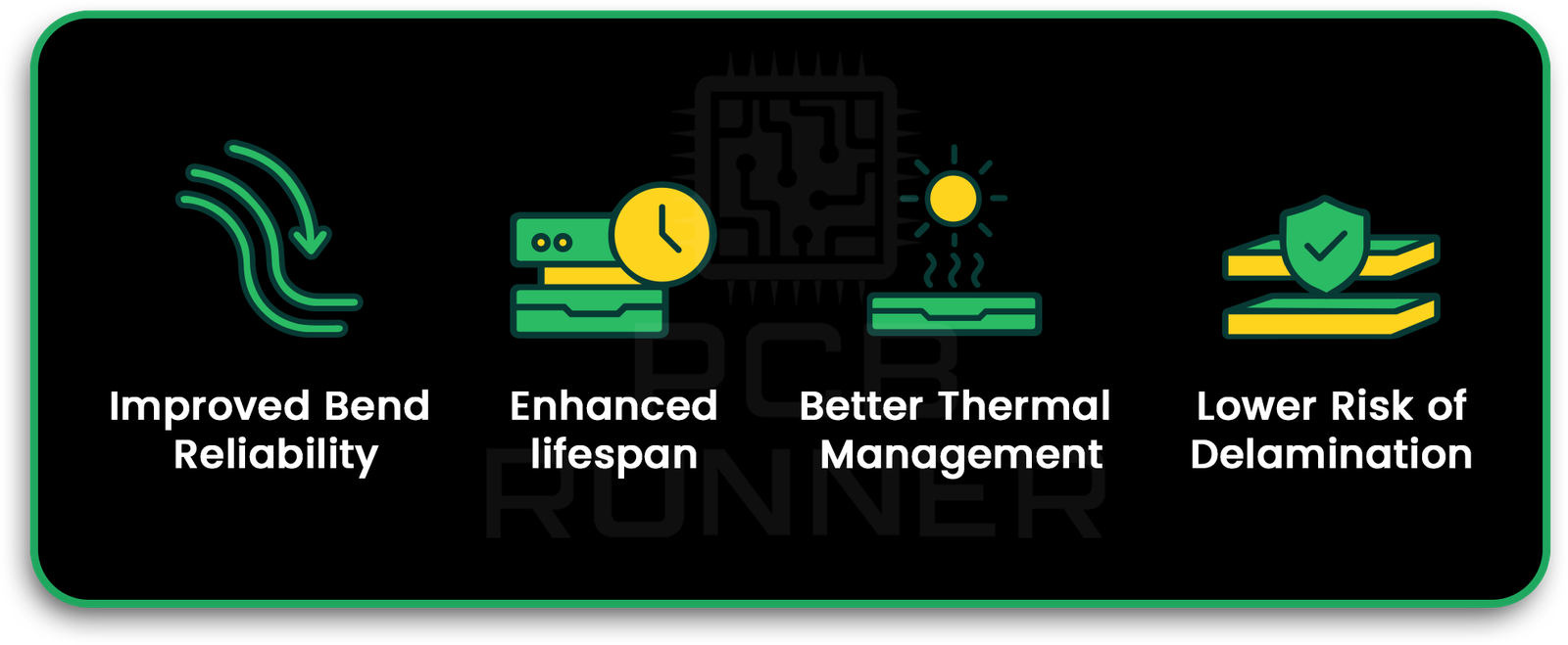
The Tg of the resin directly affects mechanical strength, dimensional stability, and bonding quality during lamination. Low-Tg pre-pregs can soften or warp when heated during lamination. Layers might become unevenly bonded as a result. The board will maintain its shape, resist delamination, and handle thermal stress with a high Tg core and pre-preg material.

How Tg Affects Core and Pre-preg Performance

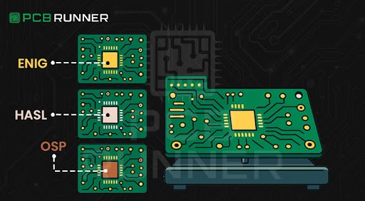
Types of Tg Materials Used in PCB Manufacturing

Standard Tg Materials (≤130°C)

These are fine for simple consumer electronics like toys or basic gadgets. They are cheaper but not built to handle high temperatures for long periods.

Standard-Tg-Materials-≤130°C

Mid-Tg Materials (130–170°C)

These materials work well in industrial or automotive products where boards face moderate heat. They strike a balance between cost and durability.

Mid-Tg-Materials-130–170°C

High-Tg Materials (>= 170 °C)

High-Tg materials are commonly used in defence, aerospace, and high-performance computing applications. They can handle multiple soldering cycles as well as high-speed signals and mechanical strain with no problem. A majority of manufacturers of printed circuit boards in Europe use high-Tg laminates to ensure longevity and reliability.

High-Tg-Materials-_-170-°C

The Effects of Tg’s on PCB Properties

Dimensional Stability

A higher Tg material maintains dimensional stability at elevated temperatures. This stops copper traces or connections from shifting or bending off-centre.

Lamination Quality and Delamination

Low-Tg materials may delaminate during soldering or lamination due to resin softening. Good Tg guarantees a solid bond between the layers, and also prevents the entrapment of air or gaps.

Soldering and Assembly Tolerance

If components have soldered on, the heat generated can cause boards with low Tg to crack. This issue, also known as the tombstone defect in PCB assembly, occurs when one end of a surface-mount component lifts during soldering. Low-Tg materials can worsen the tombstone soldering defect by allowing minor warping under reflow heat. High-Tg boards help prevent these issues.

Electrical Performance

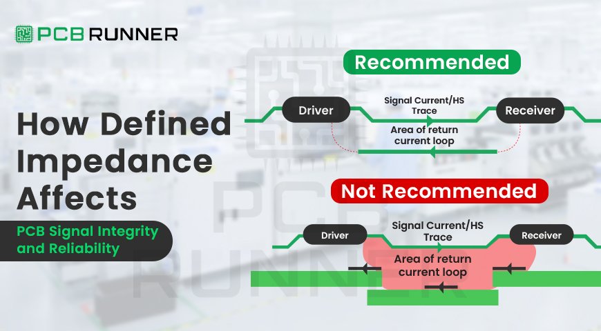
Higher-Tg materials tend to maintain stable dielectric properties under heat, supporting consistent signal integrity. It can help prevent signals from being lost as well as short circuits and leakage currents, particularly in high-frequency or high-density circuits.

Tg. CTE and Thermal Expansion – How Do They Connect

What is CTE? ( Coefficient of Thermal Expansion)

CTE is the measure of how much a substance increases when it is heated. Different PCB materials expand at different rates when heated, which creates mechanical stress between layers.

The reason why matching CTE is Important

When the thickness of the layer and its CTE don’t align, the laminates could slide away from one another in the course of cooling and heating. Choosing materials whose CTE values are well-matched minimises expansion mismatch and reduces the risk of layer separation. This means fewer cracks and more reliability of your circuits.

Selecting the Right Tg for Your PCB

Factors That Affect Tg Choice

The best Tg will depend on a couple of essential elements:

  • The maximum temperature your device can reach during its time of operation
  • The number of thermal cycles the board will experience
  • Design and thickness of the board complexity
  • Environmental factors like vibration, humidity, as well as contact with the elements

When to Select High-Tg Materials

Make use of high-Tg materials for PCBs that undergo lead-free soldering that requires greater temperature reflow. Also, opt for it if your device is over a long period of time or has a variety of fine-pitch parts.

UK PCB manufacturers for automotive and industrial sectors typically use high-Tg materials due to the consistent heat loads and lengthy operating times.

 At PCB Runner, our sales engineers are there to help you select the ideal Tg materials for your application by balancing cost, performance, and manufacturability at sales@pcbrunner.com

Test and Measurement of Tg PCB Materials

How Tg Is Measured

Engineers employ tests such as Differential Scanning Calorimetry (DSC) and Thermomechanical Analysis (TMA) to determine the Tg. These tests gradually heat the material and monitor its physical or dimensional changes to identify the glass transition point.

Why Consistency Matters Between Suppliers

Two different suppliers might list the same Tg in their products; however, slight variations could still be present. A difference of 5-10 degrees Celsius could affect the reliability of the board. Make sure you check the Tg value prior to mass production to prevent surprises in the future.

Common Issues from Wrong Tg Selection

Using materials with the wrong Tg can cause serious manufacturing issues:

  • Tombstone issue and soldering problems
  • Layer separation or delamination
  • Cracked vias due to uneven expansion
  • Reduced reliability under high temperatures

However, using materials with improper Tg can indirectly increase the likelihood of the tombstone defect by altering how heat distributes across the board. Inconsistent reflow profiles or laminate stress can amplify the tombstone effect PCB during assembly.

How to Ensure Proper Tg Handling During PCB Manufacture

Connect with Tg Requirements for Fabricator

Be sure that the fabricator is aware of your desired Tg requirements when you are designing the layout. This allows them to select the correct materials and profiles for lamination.

Control Lamination Temperature and Duration Carefully

Rapid heating or cooling can create internal stresses that weaken the resin bond. The controlled temperature keeps Tg values in check throughout the bonding process.

Do not use multiple thermal cycles.

Reduce the number of times the board gets heated during the process of manufacturing. Fewer cycles means greater Tg retention and better layer stability.

Utilise trusted material suppliers

Choose trusted suppliers that test and validate their products. Companies such as PCB Runner confirm the quality of the laminates they employ to ensure accurate and consistent Tg ratings during production.

Technology and Emerging PCB Technologies

As electronics develop, PCBs must be able to handle higher power and have faster speeds. High-Tg materials are increasingly essential in electric vehicles, renewable energy systems, and 5G electronics.

Certain new materials contain the advantages of high Tg along with low dielectric losses to help design engineers process signals more quickly and with less heat accumulation. Europe’s PCB manufacturing industry is continuing to develop new materials to meet the increasing technical requirements.

Conclusion

The term “tg” may look like another technical word, but it plays a significant role in the performance of your PCB. It determines how well your board handles heat and soldering throughout its lifetime. A PCB made with the right Tg materials maintains its shape, bonding strength, and electrical performance under demanding conditions.

For designers, engineers, and production teams from Europe, knowing Tg can mean lower defects, more streamlined assemblies, and greater reliability. Collaboration with trusted partners like PCB Runner ensures each stage of the PCB manufacturing procedure is executed using the correct materials and a carefully controlled temperature.

By managing heat distribution, choosing appropriate Tg materials, and controlling reflow profiles, manufacturers can minimize common soldering issues such as the tombstone defect and tombstone soldering defect. Awareness of how Tg interacts with soldering temperature helps prevent the tombstone defect in PCB assemblies and improves yield across production.

FAQs

Q1: What is Tg in PCB manufacturing, and why do printed circuit board manufacturers care about it?

Tg is the temperature at which the PCB base material changes from solid to soft. Printed circuit board manufacturers consider Tg essential because it guides how well the board will handle heat during production and use.

Q2: How does low Tg lead to the tombstone defect in PCB assembly?

Low Tg materials may warp during reflow soldering, causing parts to lift or shift. This leads to the tombstone soldering defect, where one side of a small component stands up instead of sitting flat. Engineers also refer to this as the tombstone defect in PCB assembly or tombstone effect PCB, both describing the same lifting issue caused by uneven heating.

Q3: How is Tg tested during PCB production in the UK?

In PCB production in the UK, Tg is tested using heating analysis tools that show how the material reacts to temperature changes. The readings ensure consistency and reliability before boards go into assembly.

Q4: What happens when a PCB’s Tg is too low for its application?

A board with low Tg can suffer from delamination, warping, cracking, and poor soldering results. It can also experience the tombstone defect during assembly if heating isn’t well-controlled.

Q5: Why do European printed circuit board manufacturers prefer high-Tg materials?

High-Tg boards are durable, dimensionally stable, and can handle demanding environments. This is why European printed circuit board manufacturers use them in automotive, aerospace, and power systems.


Thermal Vias in PCBs

Thermal Vias in PCBs: Importance, Design Tips & Best Practices

If you build or design printed circuit boards, you already know one tricky part of the job, keeping things cool. Heat buildup is one of the biggest challenges in PCB design. When it’s not handled right, it reduces the performance and lifespan of components. That’s where thermal vias come in.

PCB Runner, a trusted PCB manufacturer in Europe, understands that good thermal management starts at the design stage. Let’s explore why thermal vias matter, how they work, and what your design choices mean for heat control, cost, and reliability.

Why Thermal Vias Matter

Let’s start with what happens inside your board. Every electronic component generates heat. Small power regulators, LEDs, high-speed chips, each one adds to the total temperature rise. The problem is that typical PCB materials like FR-4 don’t move heat very well. So, without a proper path for heat to flow, it just sits there, slowly damaging your board.

Thermal vias act as vertical heat pipes that carry excess heat from the top layer down to copper planes or heat sinks. In simple terms, they create a low-resistance thermal path so the heat can move freely.

When designed correctly, thermal vias:

  • Reduce temperature spikes around components
  • Prevent delamination and solder joint fatigue
  • Improve thermal conductivity across layers
  • Help your board last longer under load

That’s the practical side of heat dissipation in PCBs, and it’s why so many PCB fabrication projects in Europe now treat thermal design as a core step in layout.

Why Thermal Vias Matter

The Nature of Heat in PCBs

When components draw current, they release energy as heat. This heat travels through copper and laminate layers before reaching the surface or external cooling systems. But different materials have different thermal conductivities, copper is good, epoxy resin not so much.

That mismatch is why localised “hot zones” appear. Over time, these hotspots can cause warping, trace damage, or even electrical drift in precision circuits. The solution is a controlled thermal path, and vias offer precisely that.

The Nature of Heat in PCBs

Role of Thermal Vias in Heat Dissipation in PCBs

Think of thermal vias as metal straws inside your board. They connect the heat source on the surface to the inner copper layers that spread it out. The more vias you have, the easier it is for heat to find a way out.

Designers often place them under power devices like MOSFETs or voltage regulators, and in LED modules where light output can drop with rising temperature. Arrays of small vias do the job far better than one or two large ones. That’s because multiple contacts distribute heat more evenly.

PCB Runner’s engineering team is here to create thermally balanced designs for complex assemblies so contact our sales engineers today at sales@pcbrunner.com

Role-of-Thermal-Vias-in-Heat-Dissipation-in-PCBs

Impact on Reliability and Performance

Good PCB thermal management keeps the board at a stable temperature, which means your components stay within safe operating ranges. When parts run cooler, they behave predictably and have longer service lives.

On the flip side, neglecting thermal vias can create performance issues like signal distortion, expansion stress, or even component detachment. Temperature swings also weaken solder joints, a common reason why devices fail after only a few months.

Simply put, keeping the board cool keeps your product dependable.

Cost and Manufacturability Considerations

Adding hundreds of tiny vias might sound like it drives up costs, but here’s the thing, it often saves money later. Repairing a failed product costs far more than adding vias during the design phase.

A skilled PCB manufacturer in Europe will balance thermal performance with manufacturability. Drill size, spacing, plating thickness, and the number of layers all affect how easily those vias can be fabricated without adding delays or defects.

So, when designing your board, talk to your fabricator early. Their input can help you get the thermal results you want without overspending.

Types of Thermal Vias and When to Use Them

Standard Through-Hole Vias

These go from the top to the bottom of the board, carrying heat across every layer. They’re reliable, cost-effective, and widely used in high-power boards.

Via-in-Pad Vias

Here, the via sits right inside the component pad. This design helps transfer heat directly from the device to the copper layer underneath. It’s great for compact layouts where space is tight.

Micro Vias

Micro vias connect only between adjacent layers. They’re common in HDI (High Density Interconnect) designs and are effective where board thickness limits deeper drilling.

Filled or Capped Vias

Some vias are filled with copper or resin and then capped. This keeps solder from leaking during reflow and ensures a smooth surface for assembly.

When Vias Are Less Effective

They won’t help much if the board lacks solid copper reference planes or if the vias are isolated from primary power traces. You always need good thermal connectivity for them to work.

Types of Thermal Vias and When to Use Them

Key Design Guidelines for Thermal Vias

Let’s break it down with clear, practical tips you can apply to any project:

Key Design Guidelines for Thermal Vias

1. Place Vias Close to Heat Sources

The shorter the distance between the source and the via, the better. Put them under chips, near resistors, or along MOSFET legs.

2. Choose the Right Size and Aspect Ratio

Vias that are too small trap air pockets, which reduce heat flow. Use drill sizes around 0.2 to 0.3 mm and keep the aspect ratio within your fabricator’s limits.

3. Use Multiple Vias Instead of Fewer Big Ones

An array of small, evenly spaced vias improves thermal conduction more than a few large ones.

4. Connect to Copper Planes and Sinks

Always tie vias to ground or internal copper planes. More copper equals more thermal mass, which helps spread and absorb heat.

5. Plan Your Layer Stack-Up Early

You can’t fix thermal routing after the final layout. Define where the heat will flow and how inner layers share it early on.

6. Pick the Right Materials and Copper Weight

High-Tg laminates and 2 oz copper layers are common for boards that run hot. These materials handle thermal cycling better during operation.

7. Decide Whether to Tent or Plug Vias

Tenting keeps solder from entering the via. Plugging with epoxy or filling ensures a smooth surface when mounting components.

8. Verify with Simulation

Many PCB manufacturers in Europe use thermal simulation tools to check temperature distribution. If you have access to these tools, use them to visualise how your layout behaves before PCB fabrication.


Best Practices for Implementation

Start with thermal planning before you begin routing. Once the layout is done, it’s hard to go back and add proper cooling paths.

Combine your thermal vias with other cooling solutions like thermal pads, heat sinks, or fans. The goal is steady temperature, not just temporary fixes.

Work with your fabricator’s design guidelines so that what you create can actually be built. A manufacturable board saves both time and rework.

Always keep testing in mind. Leave some open zones for thermal probes and inspection points. Clear documentation of your thermal via strategy also helps the fabrication team understand your priorities.

Our design experts at PCB Runner help you validate your thermal strategy with in-depth simulation and DFM analysis.

Common Pitfalls You Should Avoid

Even experienced designers run into problems with thermal vias. Here are some you can sidestep:

  • Using too few vias under power packages
  • Forgetting to connect vias properly to inner planes
  • Ignoring the layer copper thickness while planning the heat flow
  • Placing vias so close that drilling becomes unreliable
  • Failing to label filled or tented vias in the PCB fabrication notes

Each one can slow down production or cause heat issues later. Catching them early can save entire batches from scrap.

Quick Review Checklist Before Submitting Your Design

Before sending your files to your PCB manufacturer in Europe, check these points:

  • Thermal vias under key heat-generating parts
  • Appropriate number and spacing of vias
  • Correct via fill or tenting details noted in drawings
  • Strong copper connection from via barrels to planes
  • Completed thermal simulations or test results attached

This final pass helps catch mistakes that software tools might miss.

Conclusion

Thermal vias might be tiny, but they make a big difference in how well your PCB handles stress and heat over time. When planned with care, they keep your design stable, safe, and long-lasting.

PCB Runner has built its reputation in the UK and across Europe by helping designers improve reliability through smarter heat control. Whether you’re developing power electronics, LED drivers, or compact IoT boards, smart thermal via design ensures your PCB stays calm, efficient, and ready for the field.

In the end, good thermal management isn’t about adding a few vias. It’s about thinking ahead, choosing materials, patterns, and fabrication methods that work together for the long run.

FAQs

  1. What do thermal vias do in PCB fabrication in Europe?

They transfer heat from components to internal copper layers or heat sinks, helping manage temperature during PCB fabrication in Europe. That improves performance and reliability.

  1. How many vias should I use for heat dissipation in PCBs?

That depends on component size and power level. A PCB manufacturer in Europe often recommends several small vias under each hot component for steady temperature control.

  1. Can poor via design in PCB layouts cause failure?

Yes. If the vias are too small, too few, or not connected to copper planes, heat can’t escape properly. This weakens solder joints and reduces lifespan.

  1. Does adding thermal vias increase the cost of PCB fabrication?

Slightly, but it’s worth it. The added cost during fabrication is small compared to the savings from improved reliability and fewer failures.

  1. What materials improve PCB thermal management in Europe?

High-Tg laminates, aluminium-backed boards, and thick copper layers are all good choices for better heat dissipation in PCBs made by manufacturers in Europe.


Pin 1 Orientation

The Importance of Pin 1 Orientation for Reliable PCB Assembly

In the world of modern electronics, precision defines success. Even the smallest component misalignment can compromise the performance of an entire circuit. Among the most overlooked details in board design and manufacturing is Pin 1 orientation, a crucial factor in ensuring accurate assembly, reliable operation, and long-term functionality.

If you’ve ever been involved in Design for Assembly (DFA), PCB assembly services, you’ll know that the correct identification and placement of Pin 1 is key to avoiding costly errors. Whether it’s a microcontroller, connector, or integrated circuit, a single misplaced component can lead to short circuits, reversed connections, or complete board failure.

Let’s explore why Pin 1 orientation is so important, how it affects the quality of your build, and the best practices that help manufacturers get it right every time.

At PCB Runner, we emphasize the importance of correct orientation at every stage from design through turnkey PCB assembly ensuring your products meet performance and quality standards.

What is Pin 1 Orientation and Why is it Important?

Every component on a printed circuit board (PCB) has a specific way it must be placed. The “Pin 1” mark identifies the starting point of a component’s connection pattern. On ICs, connectors, or headers, this mark tells the assembler which way to align the part on the board.

When the Pin 1 orientation is incorrect, signals travel through unintended paths, leading to functional issues and potential component damage. In surface-mount and through-hole components alike, incorrect placement can also make soldering inconsistent and cause rework delays.

In short, clear marking and consistent handling of Pin 1 orientation are the foundation of reliable turnkey PCB assembly operations.
Pin 1 Orientation

The Role of Design in Correct Orientation

The first step in ensuring proper Pin 1 placement begins during the PCB design stage. Engineers must clearly define orientation indicators within the layout software. This often includes silkscreen markings, pin numbering, or specific pad shapes that visually guide assemblers.

CAD libraries should include standardised component footprints that clearly denote Pin 1. It’s good practice for design engineers to maintain consistent labelling conventions across all components, as it minimises the risk of confusion later during manufacturing or inspection.

Some additional design practices that improve orientation reliability include:

  • Adding fiducial marks for camera alignment in automated system

Adding fiducial marks

  • Including Pin 1 notches or dots in the silkscreen.

 Pin 1 notches

  • Cross-verifying footprints before finalising Gerber files.

Cross-verifying footprints

Even with automation and inspection tools, clarity at the design level remains critical for preventing assembly errors.

How Pin 1 Orientation Impacts Automated Assembly

In automated PCB assembly tips, proper orientation is vital to smooth production flow. Pick-and-place machines depend on optical recognition to position components precisely on the board. If the Pin 1 mark is unclear or inconsistent, the equipment may rotate or misplace the part.

When this happens, production lines must be stopped to correct the issue, increasing downtime and rework costs. Repeated mistakes can also reduce overall yield and delay project timelines.

Additionally, when it comes to surface-mount technology guide practices, solder paste application and reflow temperature profiles rely heavily on correct part orientation. Incorrect alignment can cause bridges, tombstoning, or cold joints, all of which compromise the reliability of the finished product.

PCB Runner ensures reliable results with advanced quality checks at every stage contact our sales engineers at sales@pcbrunner.com

Common Mistakes That Lead to Orientation Errors

Despite clear industry standards, Pin 1 orientation errors still occur for several reasons:

  • Inconsistent footprint libraries where the Pin 1 indicator is missing or mislabelled.
  • Ambiguous silkscreen symbols that confuse manual assemblers.
  • Incorrect rotation settings in pick-and-place programming.
  • Human oversight during visual inspection or manual placement.

Simple preventive measures such as design audits, automated optical inspection (AOI), and staff training can help avoid these common pitfalls.

Best Practices for Reliable Pin 1 Orientation

Ensuring correct Pin 1 alignment requires cooperation between design, manufacturing, and quality control teams. Here are some widely adopted practices:

  • Use clear silkscreen markings: Every component footprint should visibly indicate Pin 1. Adding a small dot, notch, or arrow on the board helps both automated systems and human assemblers quickly identify orientation. Consistent markings across all boards also make inspection faster and reduce placement errors during production.
  • Standardise component libraries: Maintain a unified design database across all projects. When every designer works from the same verified footprint library, inconsistencies in Pin 1 indication are eliminated. This approach improves communication between design and assembly teams while reducing time spent on rework or clarifications.
  • Verify with visual inspection: Always double-check component placement before soldering. A quick inspection stage using AOI (Automated Optical Inspection) or manual review helps catch misaligned parts early. Detecting orientation errors before reflow saves costs, materials, and prevents functional issues in the final assembly.
  • Cross-reference pick-and-place data: Ensure machine orientation data matches the design file. Verifying this alignment before the assembly run prevents misplacement of components during automated mounting. It’s also a good habit to review the rotation parameters defined in the CAD software and machine program for consistency.
  • Train assembly staff: Clear communication between engineers and technicians prevents confusion. Regular training sessions on reading orientation marks and interpreting PCB layouts can significantly reduce assembly mistakes. When the whole team understands the importance of Pin 1 alignment, overall production reliability improves.

How PCB Runner Maintains Orientation Accuracy

Companies like PCB Runner integrate precision and process control into every step of the assembly workflow. From automated placement to AOI verification, each board passes through multiple quality checks that ensure components are oriented correctly before soldering.

Their experience in handling complex assemblies helps ensure that clients receive dependable results, especially when working with fine-pitch components or mixed-technology layouts. Consistency in Pin 1 orientation directly contributes to overall production efficiency and product reliability.

The Connection Between Pin 1 and Overall Board Performance

Although it may seem like a small design detail, the position of Pin 1 can influence overall board integrity and signal performance. Misalignment often results in reversed polarity or crossed signal paths that can lead to data errors or component failure.

In high-speed or high-density designs, where precise trace routing is essential, even a slight error in orientation can disrupt impedance control and introduce unwanted noise. Ensuring accuracy from the start prevents such performance degradation and extends product lifespan.

Conclusion: Getting the Details Right

In PCB assembly, reliability comes from paying attention to detail. The orientation of Pin 1 is one of those seemingly minor factors that can make or break the success of a design. Correct alignment ensures that signals flow as intended, components perform efficiently, and the finished board meets its expected lifespan.

PCB Runner maintains orientation accuracy to help manufacturers and engineers achieve reliable results. Whether you are working with complex prototypes or large-scale production, ensuring proper Pin 1 placement through trusted PCB assembly services and verified processes will always be a critical part of achieving consistency and quality in your builds.

Multi-layer-Semi-Flex-PCB

Multi-layer Semi-Flex PCB Design: How Airgaps Improve Durability and Bend Performance

Innovation in electronics often comes from subtle yet impactful design improvements. One such advancement is the multi-layer semi-flex PCB design, a hybrid solution that combines the rigidity of traditional boards with the flexibility needed for dynamic applications.

If you’ve worked with flex PCB production, you’ll know that semi-flex boards are designed for devices requiring controlled bending during assembly or operation.

They are useful in applications where space is limited and reliability is essential, such as in automotive electronics, industrial equipment, and medical devices.

multi-layer semi-flex PCB design

What Exactly Is a Semi-Flex PCB?

A semi-flex PCB is a rigid printed circuit board that includes the flex layers capable of bending. This is achieved by carefully stacking the thin flex Polyimide layers in targeted layer sequence to meet required bandability.

Semi-Flex PCB

Unlike a fully flexible PCB, a semi-flex design does not require additional connectors or separate flexible layers. This simplifies the assembly process, reduces overall costs, and minimises potential points of failure. It strikes an ideal balance between flexibility and structural strength.

Looking to optimize your next flex PCB production project?

PCB Runner provides custom semi-flex PCB manufacturing with precise engineering and reliable turnaround times. Submit your design files at sales@pcbrunner.com for review and pricing 

The Role of Airgaps in Semi-Flex PCB Design

The inclusion of airgaps has significantly improved the performance and reliability of semi-flex PCBs. An airgap refers to a deliberate space left between selected layers in the PCB stack-up. This feature helps distribute stress evenly when the board bends, which enhances both its flexibility and durability.

Airgaps-in-Semi-Flex-PCB

When PCB Designers need to make m rigid flex PCB bends, The stress builds up in the center of flex outer layers, which can lead to stiff curves or crack.. By introducing an airgap, the inner airgap structure between flex can absorb strain more efficiently and allow more bendradius then stacked Flex multi layers, preventing material fatigue and extending the board’s lifespan. The air gap also contributes to better thermal balance and mechanical stability.

Benefits of Airgap Integration

Adding airgaps to a multi-layer PCB design can transform how the board performs under repeated movement or stress. Here are some of the main advantages:

  • Improved bend reliability: Airgaps allow smoother bending and reduce stress concentration in the copper and dielectric layers.
  • Enhanced lifespan: Boards with air gaps can endure more bending cycles, maintaining consistent electrical performance.
  • Better thermal management: The air pocket helps dissipate heat efficiently, preventing localised expansion or damage.
  • Lower risk of delamination: By absorbing internal stress, air gaps help maintain adhesion between layers.

This innovation makes semi-flexible boards suitable for applications that require repeated movement without compromising electrical integrity.

Talk to our PCB engineering experts at PCB Runner to explore rigid flex PCB manufacturing options that match your specifications. Contact Us

Benefits of Airgap Integratio

Design Considerations for Semi-Flex PCBs

Designing a semi-flex PCB with airgaps requires precise engineering. Factors such as material selection, copper thickness, and the placement of flexible zones all affect how well the board performs.

Engineers typically use polyimide or specially treated FR4 materials to balance flexibility and mechanical strength. The bend radius must also be carefully calculated; a smaller radius increases strain, while a larger one can reduce compactness.

Working with a reliable rigid flex PCB manufacturer ensures that these aspects are optimised during production. Manufacturers can simulate mechanical stress prior to fabrication, allowing them to predict how the board will perform under real-world conditions.

Applications of Multi-layer Semi-Flex PCBs

Semi-flex technology is becoming increasingly popular across industries that demand compactness and dependability. Some notable uses include:

  • Automotive systems: Used in dashboards, LED modules, and sensor connections where limited flexibility is required.
  • Medical equipment: Ideal for compact diagnostic tools that need to handle repeated movement.
  • Consumer electronics: Found in foldable devices, cameras, and wearable gadgets.
  • Industrial automation: Perfect for control panels and robotic systems with moving parts.

Semi-flex PCBs reduce the need for connectors and separate flexible circuits, simplifying design and assembly.

Understanding the Rigid Flex with Airgap Concept

Another important innovation in PCB engineering is the rigid flex with airgap design. This method combines the advantages of rigid-flex technology with the structural benefits of airgaps.

By introducing small spaces between certain layers, the design reduces mechanical fatigue in flexible sections. This makes the pcb more resistant to bending stress while preserving its electrical performance. Engineers often use this design in high-reliability applications such as aerospace, medical devices and defence electronics.

How Flex Airgap PCBs Enhance Performance

A flex airgap PCB offers additional versatility by providing controlled flexibility where needed without compromising stability elsewhere. The air gap helps ensure that the bending area maintains its structural integrity, allowing repeated motion without cracking or delamination.

This type of PCB is particularly valuable in designs where lightweight and compact construction are essential. For example, in portable medical devices or compact industrial controllers, the air gap ensures long-term durability even under constant mechanical stress.

The Role of Stackup Engineering

In advanced designs, engineers often use a Rigidflex airgap stackup, which involves carefully layering rigid and flexible materials with integrated airgaps. The goal is to balance electrical performance, heat dissipation, and mechanical strength.

Every layer in this stackup is placed strategically to maintain signal integrity and avoid excessive stress in the bending zones. This method makes it easier to produce PCBs that are dependable and built to last, even in tough conditions.

Industry Trends and Evolving Design Practices

With electronics becoming more compact and sophisticated, designers are constantly exploring ways to combine flexibility, strength, and cost efficiency. Airgap technology is a key part of this evolution, offering better control over board mechanics without requiring exotic materials or complex assembly processes.

As manufacturing capabilities improve, semi-flex PCBs are becoming more accessible across industries. Companies like PCB Runner are continually refining techniques that ensure consistent quality, predictable performance, and long-term reliability.

As PCB Runner continues to innovate, we help clients across industries implement multi-layer semi-flex designs that deliver high performance, predictable reliability, and scalable manufacturability.

Conclusion: The Future of Semi-Flex PCB Engineering

The multi-layer semi-flex PCB design represents the next step in achieving flexible, durable, and compact electronic assemblies. Engineers can greatly improve a board’s bending performance, heat stability, and mechanical strength by incorporating air gaps. Designers looking for efficient, flexible, and reliable solutions should consider air gap integration as a better and cost-effective option.

Partnering with experienced manufacturers such as PCB Runner helps ensure every design meets precise technical standards while maintaining consistent quality throughout production.

FAQs

  1. What is a semi-flex PCB?

A semi-flex PCB is a rigid board with certain areas engineered to bend, offering flexibility without the need for separate connectors or cables.

  1. How do air gaps improve durability?

It reduces internal stress during bending, preventing cracks, delamination, and other mechanical failures.

  1. What materials are used in semi-flex PCBs?

Engineers commonly use modified FR4 or polyimide materials that balance flexibility and strength.

  1. What is a Rigidflex airgap stackup?

It’s a structure combining rigid and flexible PCB layers with integrated airgaps to improve mechanical reliability.

  1. Why are semi-flex boards preferred for modern electronics?

They reduce space, improve reliability, and simplify assembly compared to traditional rigid or fully flexible boards.

Fiducials

What Are Fiducials & Why They Became Essential for PCB Production Europe & PCB Printed Circuit Board Assembly

The foundation of every electronics today is printer circuit boards (PCBs) as they are used in everything from consumer gadgets to complex industrial systems. As PCB production in Europe and worldwide has evolved, so have the methods of ensuring precision, reliability, and repeatability in manufacturing.Among the key design features that make this possible are fiducials. These small copper markers may seem insignificant, but they play a crucial role in ensuring accuracy during PCB printed circuit board assembly

In this blog, we’ll explore fiducial in PCB, the different types available, fiducial placement on PCB guidelines, and why these elements have become indispensable for modern electronics manufacturing.

The Role of Fiducials in Modern PCB Manufacturing 

What Is Fiducial in PCB?

A fiducial in PCB is a small, accurately placed copper marker on the circuit board surface. It acts as a reference point for automated optical systems, allowing machines to recognize board orientation and position components with high accuracy. Without fiducials, high-speed assembly equipment would struggle to place in tiny SMD components correctly.

Historical Evolution: From Manual to Automated Assembly 

In earlier decades, PCB assembly was mostly manual, and alignment was guided by human operators. With the rise of surface-mount technology (SMT) and automation, fiducials became essential. By providing a universal visual reference, fiducials allowed assembly machines to align boards consistently and minimize placement errors, revolutionizing PCB production in Europe and across global markets.

At PCBRunner, our advanced PCB printed circuit board assembly processes are designed with precise fiducial recognition systems, ensuring accuracy even for high-density, complex boards. This level of precision helps our clients reduce defects and achieve faster time-to-market

Types of Fiducial in PCB Designs 

Fiducials come in different types, each serving a specific purpose depending on the complexity of the board design.

Global Fiducials 

Global fiducials are placed at the corners or edges of the board. They help machines detect the PCB’s orientation as a whole and are critical in ensuring the entire layout is aligned correctly before component placement begins.

Local Fiducials 

Local fiducials are smaller markers positioned near complex components, such as BGAs (ball grid arrays) or fine-pitch ICs. They allow machines to fine-tune alignment for a specific area, ensuring even the smallest leads or solder balls are placed accurately. 


Other Fiducial Types

In some cases, PCB designers may use custom fiducials, such as cross or hash patterns. While less common, they can help when unique geometries or extremely tight tolerances are required.

By understanding the types of fiducial in PCB, designers can apply the right strategy for both simple and complex assemblies.

Fiducial Placement PCB – Best Practices & Guidelines 

The success of PCB fiducials depends heavily on where and how they are placed. Following industry-standard fiducial guidelines ensures manufacturability and minimizes errors during production.

PCB Fiducial Guidelines 

  • Shape and size: Fiducials are usually circular, 1–3 mm in diameter, with no solder mask covering them.

Shape and size

  • Clearance: A solder mask clearance of at least 1 mm around the fiducial ensures that automated cameras can easily detect it.

Clearance

  • Surface finish: Fiducials should match the PCB’s surface finish (e.g., ENIG or HASL) to maintain visibility.

Surface-finish

When and Where to Place Fiducials

  • Global placement: At least two, preferably three, fiducials should be placed on opposite corners of the PCB.
  • Local placement: Components with fine pitch should have at least two local fiducials nearby.
  • Symmetry: Avoid placing fiducials in random positions; symmetric placement enhances machine recognition.

By following these fiducial placement PCB practices, manufacturers improve the efficiency and reliability of PCB printed circuit board assembly.

At PCBRunner, our engineering team applies IPC-compliant fiducial placement standards across every build, from prototypes to full-scale production. This ensures flawless compatibility with SMT automation, helping businesses reduce costly placement errors and maximize manufacturing efficiency.

How Fiducials Enable Reliable PCB Assembly & Production in Europe 

Automation has made PCB manufacturing faster and more precise, but it relies on fiducials for consistency.

Integration with Pick & Place Machines

Modern pick & place machines use high-resolution cameras to align boards. Fiducials act like “anchors” for these machines, allowing them to calculate the exact positioning of each component. Without fiducials, machine vision systems could misinterpret copper pads, vias, or traces, leading to misalignment.

Error Reduction and Efficiency Gains

By providing a universal reference point, fiducials drastically reduce placement errors, improve throughput, and minimize costly rework. For PCB production Europe manufacturers who face high demand for precision and quality, fiducials are non-negotiable.

Challenges, Common Mistakes & Troubleshooting in Using Fiducials

Even though fiducials are simple, mistakes in design can cause problems during manufacturing.

Overcrowding and Masking Issues 

If fiducials are too close to other copper features, or if solder mask partially covers them, machine vision may fail to detect them.

Mismatch with Assembly House Requirements 

Different PCB assembly providers may have specific fiducial requirements. Designers who overlook these guidelines risk delays, rejections, or added costs. For European production houses, adhering to IPC standards ensures compatibility across multiple assembly lines.

Summary & Future Trends in PCB Fiducials for European Production 

Fiducials might be small, but they play a vital role in the success of PCB printed circuit board assembly. By serving as precise reference markers, they enable machine vision systems to align components, reduce errors, and keep European PCB manufacturers competitive.

As PCB technology moves toward greater miniaturization and higher component densities, fiducials will continue to adapt. Future trends may include micro-fiducials designed for ultra-small components and advanced machine learning systems capable of reading boards with fewer fiducials.

In conclusion, fiducials are not just small copper dots they are the backbone of accuracy in pcb production and beyond.

Spring-Loaded Pins Enhance Connectivity

How Spring-Loaded Pins Enhance Connectivity and Reliability

Printed circuit boards (PCBs) are the backbone of today’s electronics, and printed circuit board manufacturers continually seek innovations to improve signal reliability and simplify testing. Among the most versatile interconnect components are spring-loaded pins which are also known as pogo pins, have become indispensable in pcb printing and assembly. By offering consistent contact force and exceptional durability, spring-loaded pins help engineers create more dependable connections while reducing manufacturing complexity.

The Role of Spring-Loaded Pins in Modern PCB Circuit Board Manufacturers 

In high-volume production environments, printed circuit board manufacturers need efficient ways to connect test probes, programming fixtures, and modular boards. Spring loaded pin connectors provide a precise, self-compensating contact solution that meets these demands.

  • Streamlined pcb printing and assembly: Because pogo pins can compensate for slight misalignments, manufacturers experience fewer reworks and higher yields.
  • Versatile applications: From battery contacts to charging docks and signal testing, spring electrical contacts are used across consumer electronics, automotive systems, and industrial control equipment.

 Versatile applications

  • Reduced wear and maintenance: Compared with fixed soldered contacts, spring loaded contact pins withstand thousands of mating cycles without degradation.

Reduced wear and maintenance

PCBrunner helps printed circuit board manufacturers integrate pogo pin technology directly into their workflows resulting in faster time-to-market and lower production costs.

Anatomy and Mechanism of Spring-Loaded Pins 

Understanding how pogo pins pcb work helps design teams maximize their advantages.

Components: Plunger, Barrel, Spring, Tip 

A typical spring loaded pin consists of three key parts:

  • Plunger: The movable tip that presses against the mating pad.
  • Barrel: The stationary outer casing that maintains alignment.
  • Spring: A precision coil that provides the correct contact force.

Components_ Plunger, Barrel, Spring

All are usually plated with gold or nickel to ensure low resistance and long life.

Contact Force, Stroke, Tolerance and Material Selection 

The internal spring defines the pin’s stroke the distance and the plunger travels as the contact force is required. For high-frequency or power applications, choosing the correct plating and barrel material is critical to maintain conductivity and resist corrosion over thousands of cycles.

Key Advantages: Connectivity, Durability, and Reliability 

For printed circuit board manufacturers, integrating spring loaded pin connectors brings a host of benefits:

  • Consistent electrical performance: The spring maintains stable pressure, ensuring low-resistance connections even with vibration or thermal expansion.
  • High mating cycles: Many designs exceed 100,000 insertions, far surpassing typical soldered joints.
  • Design flexibility: Whether for pcb printing test points or modular assemblies, engineers can create compact, reusable interconnects.

When you partner with PCBrunner, you not only get access to high-quality pcb printing, but also expert guidance on the right spring electrical contacts for your application.

Design Considerations when Integrating Spring-Loaded Contact Pins 

Proper design ensures that spring loaded contact pins perform to specification.

Alignment, Pad Design, and Tolerance Management

Engineers should carefully size landing pads to match plunger diameter, and maintain tight tolerance on board thickness. Misalignment or insufficient pad area can reduce contact reliability.

Mounting Options: Through-Hole vs SMT for Spring-Loaded Pin Connectors 

Depending on the application, designers can choose through-hole for mechanical strength or surface-mount (SMT) for automated pcb printing. Each method affects assembly cost and long-term reliability.

Use Cases: Where Spring Electrical Contacts Shine 

Spring-loaded technology supports a variety of B2B applications:

  • Test fixtures and programming jigs: Spring electrical contacts enable high-speed functional testing without permanent soldering.
  • Battery and charging interfaces: Portable devices, industrial scanners, and medical electronics rely on spring loaded pin connectors for quick connect/disconnect.
  • Modular and stacking PCBs: In products where boards must be removable or upgradeable, pogo pins pcb create secure but serviceable links.

These applications highlight why leading pcb circuit board manufacturers integrate pogo pins into their design toolkits.

Best Practices and Maintenance for Spring-Loaded Pin Connectors 

Although highly robust, spring pins benefit from preventive care to ensure maximum lifespan.

Cleaning, Lubrication, and Wear Mitigation 

Regular cleaning with isopropyl alcohol and applying a thin protective lubricant help prevent oxidation and wear, especially in harsh industrial environments.

Troubleshooting Contact Failures and Testing

If resistance rises or signals drop, check for debris, misalignment, or worn plating. Many printed circuit board manufacturers schedule periodic electrical testing to maintain quality.

Final Thoughts: Boosting PCB Reliability with Spring-Loaded Pins 

By combining mechanical compliance with electrical stability, spring loaded pins enable more reliable, cost-effective solutions for pcb printing and assembly. For engineers and procurement teams working with printed circuit board manufacturers, incorporating spring loaded contact pins or pogo pins pcb can simplify production, improve product longevity, and lower total cost.

At PCBrunner, we don’t just deliver pcb printing but we also provide complete solutions, including high-quality pogo pins and expert engineering support.

Ready to upgrade your connectivity? Contact us today at sales@pcbrunnner.com to discuss your project. Let PCBrunner be your trusted partner in building more reliable, high-performance electronics.

Defined Impedance

How Defined Impedance Affects PCB Signal Integrity and Reliability

In the evolving world of custom printed circuit board manufacturing, precision is everything. As data speeds increase and electronic devices become more compact, signal quality and consistency become paramount. One key factor behind reliable high-speed data transmission is defined impedance a controlled value that ensures signals travel through PCB traces without unwanted reflections or distortions.

For every pcb manufacturer in Europe or globally, maintaining defined impedance isn’t just a design choice; it’s a necessity for achieving stable PCB signal integrity and long-term reliability.

Why Defined Impedance Matters in Modern High-Speed PCBs 

With the rise of high-speed PCB design, electronic systems today must support gigabit data rates, differential signaling, and complex multi-layer structures. Impedance control ensures each transmission line (trace) behaves predictably, preventing reflections that cause signal degradation or timing errors.

Defined impedance directly affects PCB performance optimization — an incorrectly matched impedance can reduce signal amplitude, introduce noise, and even cause complete data loss. Whether in automotive radar, 5G modules, or aerospace control systems, stable impedance enables consistent performance across temperature, voltage, and manufacturing variations.

For a custom printed circuit board, impedance definition typically falls between 50Ω (single-ended) and 90Ω (differential). Achieving this consistency requires precise control over dielectric materials, copper thickness, and trace geometry.

Fundamentals of Impedance, Transmission Lines & Signal Integrity 

Understanding impedance is essential before mastering high-speed PCB design. Impedance is the opposition that a circuit presents to alternating current — in PCBs, it depends on trace width, height above the reference plane, and the dielectric constant of the substrate.

Impedance-Transmission-Lines-Signal-Integrity

Signal reflections, return loss, and mismatch effects

When the impedance of a transmission line doesn’t match the load, part of the signal reflects back toward the source, degrading PCB signal integrity. These reflections cause return loss and can distort digital waveforms, leading to data errors.

In high-speed environments, even small mismatches can create ringing, crosstalk, or EMI issues. Maintaining consistent impedance throughout the signal path helps avoid these reliability problems.

Microstrip, stripline & differential pair characteristic impedance

Different routing methods influence impedance control.

  • Microstrip lines (traces on the outer layer) have one reference plane beneath them.
  • Striplines (internal layers) have two reference planes and offer better shielding.
  • Differential pairs use two coupled traces to carry complementary signals, with an impedance typically set to 90Ω.

Selecting the right configuration is key to balancing manufacturability, cost, and PCB performance optimization.

Microstrip-stripline-differential-pair

Designing for Defined Impedance in High-Speed PCB Layouts 

The layout stage is where most impedance-related issues can be prevented. During custom printed circuit board design, engineers define trace widths, spacings, and layer stack-ups based on the target impedance.

Stack-up, dielectric constant, trace geometry considerations 

The PCB stack-up determines how signals travel between layers. The dielectric constant (Dk) of the material affects signal propagation speed — variations in Dk can cause impedance drift. To ensure stable impedance, designers must use controlled dielectric materials and consistent copper thicknesses.

Modern pcb manufacturers in Europe provide online impedance calculators and stack-up design tools that let engineers simulate impedance before fabrication, ensuring accuracy and predictability.

Via transitions, layer changes, and impedance discontinuities 

Each via or layer transition can alter the signal path’s geometry, introducing impedance discontinuities. Proper design — using backdrilled vias, anti-pads, or via stubs — minimizes these variations. Maintaining smooth transitions helps preserve PCB signal integrity, especially in differential pairs used for USB, HDMI, or PCIe signals.

High-Speed PCB Layouts

Manufacturing and Verification: Ensuring Impedance Accuracy

Even the best design can fail if manufacturing doesn’t maintain the specified impedance. That’s why collaboration between designers and a pcb manufacturer in Europe or trusted fabrication partner is crucial.

Coupon, TDR, and VNA testing methods 

During production, custom printed circuit boards often include test coupons — miniature replicas of signal traces — to verify impedance consistency. Manufacturers use Time Domain Reflectometry (TDR) or Vector Network Analyzer (VNA) testing to measure actual impedance and detect mismatches.

Tolerances, process control, and design-to-manufacturing alignment 

Impedance tolerances are typically ±10%. Maintaining them requires tight process control over etching, plating, and lamination. European PCB suppliers emphasize process repeatability and material traceability to ensure high-speed PCB design reliability at scale.

Partnering early with your manufacturer ensures your custom printed circuit board design parameters align with real-world fabrication capabilities — the hallmark of effective PCB performance optimization.

Implications for Reliability & Long-Term PCB Performance 

Stable impedance directly enhances long-term PCB signal integrity and reliability. Mismatched impedance leads to localized heating, bit errors, and premature aging of components.

When designed and verified correctly, defined impedance reduces jitter, improves timing margins, and allows faster data rates without increasing error rates. In harsh environments like aerospace or industrial systems, this translates to consistent performance even under temperature or vibration stress.

For designers, that means fewer redesigns and better end-product reliability. For any pcb manufacturer in Europe, it demonstrates technical expertise and manufacturing precision — key differentiators in the global electronics market.

Partnering with a Trusted PCB Manufacturer for Defined Impedance Control

The effectiveness of impedance control lies not only in design tools but also in collaboration. A custom printed circuit board partner who understands the nuances of high-speed PCB design can help optimize layer stacks, select materials, and test impedance during every stage of production.

Choosing a reputable pcb manufacturer in Europe ensures compliance with IPC standards, consistent process control, and transparent quality assurance — vital for maintaining signal reliability in today’s complex electronics.

Conclusion: Defined Impedance — The Cornerstone of PCB Reliability

Defined impedance isn’t just a technical parameter; it’s the foundation of reliable signal transmission and consistent performance in modern electronics. Whether you’re designing for automotive, telecom, or industrial systems, integrating impedance control during the custom printed circuit board design phase is essential for PCB performance optimization.

By working closely with an experienced pcb manufacturer in Europe, you can ensure that your design intent translates accurately to production — resulting in superior PCB signal integrity, enhanced durability, and products built for the future of high-speed communication.

Future of Electronics

The Future of Electronics: Up and Coming PCB Designs

Have you stopped to think about how your TV, phone as well and your espresso maker actually work? It’s not just about the buttons you push or the display you view. It’s the hidden components in the. One of the most crucial components in almost all electronic devices is what’s known as the printed circuit board manufacturers, or PCB for short.

An electronic circuit acts similar to the nervous system of electronics. It connects various components, resistors, sensors, etc., so that they are able to communicate with each other and enable your devices to work. Without PCBs, the current world we live in today would not exist at all.

But here’s the deal: PCB technology is changing. Like how phones became smarter and cars became more eco-friendly, PCB design and manufacturing are undergoing massive changes. If you’re looking for the latest developments in electronics, it’s essential to know what’s next.

Let’s examine the latest trends, concepts and technological breakthroughs that will shape our future design of PCBs that range from the newest materials to greener production.

Why PCBs are Evolving So Quickly

Technology moves fast. Consider how fast smartphones evolved from chunky bricks to sleek and stylish devices that can fit into your pockets. A similar speed change is occurring in the design of PCBs and their assembly.

There are several significant reasons for this dramatic shift:

  • Devices are smaller but more robust. That means we require a simple PCB circuit design that can fit many components in less space.
  • Speedier data transfer. Modern electronics require PCBs that can handle high-speed signals without causing interference.
  • Goals for greener technology. Manufacturers are seeking environmentally friendly materials, as well as energy-efficient PCB manufacturing techniques.
  • The rise of bright things. From smart fridges to wearable health trackers, every device requires a customised PCB design that is lighter, smaller, and more efficient.

This is pushing producers of printed circuit boards from the UK as well as around the globe to implement new methods.

PCBs are Evolving So Quickly

From Simple to Smart: The Changing Face of PCB Design

In the past, PCBs were relatively simple. They came with a flat board and copper paths that linked several components. But what about today?

  • We have PCBs with flex and rigid-flex that are flexible and bendable for wearable technology.
  • HDI (High-Density Interconnection) boards cram more circuits onto smaller boards.
  • Key PCB assembly services can handle everything from printing PCBs to attaching chips in one step, thereby cutting down time.

It’s similar to comparing an old chalkboard for a class to a new smartboard. The goal is the same, but the capabilities are on an entirely new level.

Emerging Trends in PCB Fabrication and Assembly

Here are a few trends you’ll need to keep in mind if you’re an electronics enthusiast:

Emerging Trends in PCB Fabrication and Assembly

  1. A) Miniaturisation and a Higher Density

Electronics are becoming smaller without dropping performance. It means PCB designers have to work with small lines and fine vias while making sure that the board is reliable.

B) Flexible and wearable PCBs

Imagine a fitness band. It must flex when you move. This is why flexible PCB printing and designs with rigid-flex shine.

C) Eco-friendly customised materials

The drive towards sustainability is also impacting prototype PCB production. Modern materials are less harmful, and some are biodegradable.

D) AI-Assisted Design of PCBs

Artificial intelligence is now helping engineers design more effective PCB layouts that are less prone to mistakes and quicker turnaround times.

E) 3D Printing on PCBs

It’s not science fiction, researchers are currently researching 3D printing on PCBs, which means designs can be transformed from concept to board in much less time.

Common Questions About the Future of PCBs

Q: Will PCBs keep getting smaller forever?

It’s unlikely to last forever, however, in the next 10 years, at the very minimum, miniaturisation will be on the rise. There’s room to squeeze more performance in a smaller space.

Q: Are custom PCB designs expensive?

Not necessarily. With the advancement of technology and automation, as well as complete PCB manufacturing, custom designs are becoming less expensive, particularly for small quantities.

Q: Is PCB printing the same as regular printing?

Not quite. As opposed to ink, PCB printing makes use of conductive materials such as copper to make electrical paths.

How Designers Keep Up

PCB fabrication and design requires the ability to think and creativity. Designers usually begin with a simple PCB circuit design and later improve it to better meet the needs of the product. They should:

  • Select the appropriate materials.
  • Make plans for signals with high speeds.
  • Check that the board is able to take on heat.
  • Make sure everything is checked prior to the prototype of the PCB.

This is the reason manufacturers of printed circuit boards in the UK frequently review designs of their customers prior to making them, as it helps avoid costly mistakes down the line.

From Idea to Product: The PCB Production Journey

Here’s a step-by-step guide on the process of making modern PCBs:

  1. Design phase: Engineers create an outline using CAD software.
  2. PCB printing: The design is printed on copper-clad boards.
  3. Etching copper that is not needed is removed, leaving the necessary paths.
  4. Drilling: Small holes are drilled to accommodate components, lead and vias.
  5. Plated surfaces and holes are coated to provide greater conductivity.
  6. Solder Mask: A layer of protection is added to protect against short circuits.
  7. Assembly: When it comes to the design of PCBs, in assembly components are soldered into place.
  8. Testing: The board is inspected to verify that it is working exactly as it was planned.

Every step is crucial. Even the most minor mistakes could cause a device to stop working.

The Role of Prototypes in Innovation

Before a product goes into production, it requires an initial PCB prototyping. This is similar to creating the prototype prior to making hundreds of devices.

Prototypes aid manufacturers:

  • Test performance.
  • Make sure that the item is in its casing.
  • Catch errors early.
  • Avoid costly errors. million tonnes

This is the reason firms invest in custom PCB designs as early as possible because it’s the base of the whole project.

Sustainability and the Future

Electronics waste is becoming a significant issue. Many old gadgets end up in landfills, and a lot of them contain hazardous materials.

The positive side? PCB manufacturers are collaborating on solutions:

  • Utilising solder without lead.
  • The creation of boards is made from biodegradable or recyclable materials.
  • It is designed for ease of disassembly so that components can be used again.

Based on the records estimates, the amount of electronic waste in the world could reach the 74 million tonne mark in 2030. A sustainable PCB design could contribute significantly to cutting down on that number.

Skills Needed for Tomorrow’s PCB Designers

As PCBs get more sophisticated, designers require new abilities:

  • Expertise in HDI and PCB fabrication using flex.
  • Knowledge of how to manage thermal in small devices.
  • The ability to design software using AI-assisted tools.
  • Be aware of the eco-friendly products and methods.

The future PCB design jobs require a combination of electronic knowledge, imagination and problem-solving.

Final Thoughts

PCBs aren’t huge, however, they’re the foundation of the electronic world. Starting from simple circuits designed for the design of PCBs to sophisticated customised PCB manufacturing, the evolution of PCBs makes devices smaller, more efficient and more cost-effective.

In the coming years, we’ll witness increasingly adaptable design, AI-driven layouts, and environmentally sustainable manufacturing methods. The result is that electronic devices will not just be more intelligent but also more considerate of their surroundings.

Although the improvements have been exciting, basic principles remain the same. Every great device begins with a top PCB.

Companies such as PCB Runner will continue to innovate, adapt and create boards that meet the requirements of the future’s technologies.


pcb-surfaces

Understanding The Best Techniques For Protecting The Surfaces Of PCBs

Have you ever wondered how PCBs (printed circuit boards) remain functional and are able to last long? The tiny copper traces on PCBs are well protected and do not corrode due to oxidation because of surface protection techniques. In this article, we will undertake a friendly, detailed exploration of PCB finishes, including what they are, their importance, and which might be most suitable for your project or learning.  

Why do PCBs require Surface Protection?  

Think about baking cookies and leaving them exposed to the open air. In no time, they become hard and stale. PCBs also contain copper and thus undergo a baking-like process. During the CNC milling process, oxidised copper will be challenging to use, similar to brown and oxidised apples stuck turning brown, which creates problems during the PCB printed circuit board assembly, as well as the final steps of assembly.  

In order to make PCBs dependable and straightforward to assemble, manufacturers apply surface finishes or specialised coatings to PCBs, which reduce the chances of air, precipitation and other dangerous things, can severely damage their performance. Manufacturers try to use surface finishes that will add to the dependability of the PCBs.

How Does The Surface Finish Of A PCB Work?  

Think about if your school locker had a shiny sticker on it that prevents it from rusting. Surface finishes on PCBs help to prevent copper from oxidising, aid in the soldering of parts onto the board, and help in the overall working of the board.  

Three of the most common finishes you’ll hear about are ENIG, HASL, and OSP.  

Exploring The Main Types Of Surface Finishes Used On PCBs  

1. ENIG: Electroless Nickel Immersion Gold Surface Finish PCB  

The surface finish ENIG is a flat surface finish of nickel and gold that is shiny and helps to waterproof a PCB. The surface is flat and shiny while also being very reliable.

ENIG-Electroless-Nickel-Immersion-Gold-Surface-Finish-PCB

Benefits:  

  • Parts soldered to the PCB will remain attached through the entire building process.
  • Best for small spaces and parts, like in a smartphone and medical tools and equipment.
  • The gold surface delays any rust for months, and in some cases, even up to a year.
  • Good for the environment and products with strict safety standards.
  • Flexible and helps in rust resistance.

Drawbacks:

  • Cost: The finishing touch on a product with gold is prohibitive.
  • Not always needed: The gold finishing touch provides needless protection on simple boards.

When to choose it?

ENIG is a good choice when you want to augment the durability and longevity of the circuit board, also if you want to solder small parts while being concerned with the safety of the circuit board and the electronics.

2. HASL: Hot Air Solder Levelling PCB Surface Finish

HASL is an older but still proper technique. It is akin to a PCB being dunked into a bath of solder. The PCB is then soldered with hot air to smooth the finish. The finishing touch can be leaded or non-leaded.

HASL-Hot-Air-Solder-Levelling-PCB-Surface-Finish

Benefits:

  • Cost-effective: This is better for a project that needs to make and sell many boards.
  • Electronic components’ protection: The copper parts of the circuit board are covered in solder, preventing rust.
  • Error identification: The shiny sensor assists in looking for cracks and the mistakes that come along with it.
  • Embraced for a long time: This has been used widely in areas such as automotive, industrial and many more industries.

Drawbacks:

  • Not super smooth: The board’s surfaces, which have copper parts, can be covered in solder, preventing rust. Also, the copper components having a rough surface to them are not advantageous.
  • Non-leaded option isn’t eco-friendly: This has left a mark on the current eco-friendly approach that many companies aim towards.

When is HASL most suitable?  

For simple projects, bigger pieces, or when the budget is tight, HASL works best. PCB circuit board manufacturers typically prefer it due to its ease of application and consistency.  

3. OSP: Organic Solderability Preservative PCB Surface Finish  

OSP surface finish PCB applies a nearly invisible organic coating. It’s like applying an evident seal to your school books, protecting them from damage. 

 OSP Organic Solderability Preservative PCB Surface Finish

Advantages:  

  • Streamlined: Cheaper than using metallic finishes.  
  • Eco: Does not contain harsh chemicals or metals.  
  • Best for flat designs: The surface is even and smooth.  
  • Repairable: Parts can be unsoldered and re-soldered without much hassle.  

Disadvantages:  

  • Limited lifespan: Protects the copper for only 6–12 months.  
  • Risk of damage: Can be easily scratched with improper handling.  
  • Hard to check off: Because it’s clear, flaws become difficult to check.  

Best for:  

The best fit for projects needing faster assembly or low-cost outsourcing with a strong focus on saving money and eco-impact.

How Surface Finishes of a PCB Change Real-Life Projects

Imagine a student crafting a model volcano for a science fair. If he doesn’t waterproof the model, it will get easily destroyed. Surface finish protects printed circuit boards the same way finishing a model volcano protects it. It helps to prevent damage, wear, and finish wear and ensures the circuit board survives thorough testing as well as use.  

Whether it is computing, robotics, medical instruments, or toy designing, the relevant pcb surface finish will enable the device to perform optimally. This is precisely why engineers and PCB manufacturers put extra thought into every decision:

  • Durability: Will the board need to endure harsh conditions for years?  
  • Solderability: Are you using parts that are smaller for the smart gadgets?  
  • Cost/ Eco-friendliness: Is the project a school project, or is it a heavy-duty industrial device?  
  • Ease of assembly: Will they need to fix or solder the board again?  

Tips to help you choose the Right Surface Finish  

  • Check the complexity of the board: Small parts and intricate circuits call for the use of ENIG. Bigger and simpler components can use HASL or OSP.  
  • Keep the expense in mind: HASL is the next cheaper after OSP, and then ENIG.  
  • Think about the shelf life of your project: ENIG survives for the longest, and then HASL can survive for a few months. OSP survives the shortest.  
  • Think of these ENIG and OSP are eco-friendly, and they are prioritising the project directly helps the environment.
  • Inspectability: Inspection of HASL is straightforward and visually accessible, while OSP is challenging to see.

FAQs

If no finish is applied to a PCB, what is the most likely outcome, and what is the gloss and matte finish for the identical PCB?

The risk is the same as an insufficient protective coating. Heating and ignoring protective etiquette risks failure. Assembly failure is like the breakdown of a bicycle left outside to rust.

Which of the described finishes has the most extended operational life, and what is the 

difference between matte and gloss finishes?

Gloss finishes are generally valued for being visually appealing compared to matte. They are more prone to scratching, so their operational life will depend on the surface treatment of the substrate.

What do I do if a joint has to be reworked?

Finishes on OSP boards are the most permissive, and so they can be worked on repeatedly, allowing easy removal of the finish and addition of solder.

Easy Ways to Remember the Differences

  • ENIG: “Gold standard”—best for tiny, long-lasting boards.
  • HASL: “Budget pick”—classic, shiny, great for bigger, less-packed boards.
  • OSP: “Green choice”—cheap, environmentally kind, but not for use after a long shelf life.

Wrapping It Up  

In creating or configuring any device, safeguarding the PCB is as critical as deciding on its contours or the components it should house. Industry Standard Surface finishes ENIG, HASL, and OSP serve as the outer guard for the circuitry, making sure it is well protected, rugged, and ready for integration, regardless of what you intend to construct.  

Depending on your expectations, expenditures, and timeline, the finish selection varies. ENIG caters best to high-density and high-end boards, HASL is beneficial to generic works, and OSP is the cheapest of the three and environment friendly.  

The good thing is that knowing these protective methods enables you to engage meaningfully with PCB circuit board vendors or design and execute projects as a seasoned professional.  

Keep in mind, every PCB, regardless of the complexity, merits the right protective finish for its intended voyage. PCB Runner stands by this philosophy, ensuring each board, regardless of its dimensions, contributes to a bright, dependable, and safe future for electronics.


PCB Trace Width and Spacing Decisions

Essential Guidelines for PCB Trace Width and Spacing Decisions

Have you thought about the reasoning behind the differences in thickness among the copper lines on printed circuit boards (PCBs)? The thicker and thinner copper lines are referred to as PCB traces. Similar to the way roads in a city transport vehicles, traces on a PCB transport electrical signals. The thickness of these traces and the distance between them significantly influences the effectiveness of PCB design.

While the majority of you might not be deeply interested in electronics, PCB printed circuit board assembly, or the processes behind a circuit board supplier in the UK, you are likely to notice that there are design rules and restrictions that need to be observed during board construction. In this blog, we will explain these rules and design restrictions for you in a way that can be easily digested, even for a beginner.

PCB Trace Width and Spacing Decisions


Why Does PCB Trace Width Matter?

Consider a PCB trace to be a water pipe. A narrow pipe will not be able to transport water easily, similar to the way a narrow trace will impede the flow of electrical current due to resistant heat. Excess heat can damage the board.

For this reason, PCB designers order the current capacity of the PCB trace width before finalizing the width of the trace. Choosing the right trace width keeps the PCB functional and ensures all signals are processed efficiently.  

Key reasons why trace width matters:  

  • Heat control – For the efficient handling of current, wider traces are less prone to overheating.  
  • Signal quality – Correct trace width minimizes noise and interference.  
  • Durability – Damage to the copper during PCB production in the UK is minimized.  
  • Compliance – Manufacturing and safety standards are met.

PCB Trace Width Matter

What Is PCB Trace Spacing and Why Is It Important?  

As with roads, traces on a PCB require distance between lanes, which in this case is called trace spacing. If lanes are too closely spaced, vehicles may collide. On a PCB, with traces spaced too closely, electrical signals may “leak” between traces. This effect, called crosstalk, can lead to short circuits.  

Good spacing:  

  • Refrains from creating shorts and sparks between signals.  
  • Reduces interference between signals.  
  • Helps meet safety regulations for high-voltage designs.  

These spacing rules are determined largely by the voltage level and the PCB production method utilized in the UK.

How to Determine PCB Trace Width

There is no need to make estimations as there are tools such as a pcb trace width calculator which will do the job for you. These calculators take into consideration:

  • The Current (Amps) the trace will carry
  • The copper thickness on your board
  • The temperature rise you can allow

Take for example a 1 amp trace. With 1 ounce copper thickness, calculators will help you determine the width to keep it safe.  

Tip: Safety margins should be added. Wider traces will accommodate for surges just like wider roads which are better equipped for uncontrolled traffic increases

Determine PCB Trace Width

How to Decide PCB Trace Spacing 

As a rule of thumb, the amount of space is to do with voltage preventing a jump. The higher the voltage, the greater the distance.

There is a common standard:

  • Low voltage (<30V): 0.1 mm spacing is often fine.
  • Medium voltage (30V–100V): 0.6 mm or more.
  • High voltage (>100V): Several mm, always comply with safety standards.

Factors Affecting PCB Trace Width and Spacing

Every printed circuit board (PCB) is unique and requires specific factors to be considered when designing PCB traces. These include:  

Current Capacity  

A trace must be ‘wider’ to manage ‘more’ current.  

Copper Thickness  

A thicker copper layer is able to manage more current without overheating.  

Voltage Levels  

More spacing is required for higher voltages.  

Signal Type  

High-speed signals require careful width and spacing to avoid cross talk.  

Environmental Conditions  

Will the PCB be exposed to high temperatures or moisture? That requires wider traces and larger spacing.  

Factors Affecting PCB Trace Width and Spacing

Using PCB Trace Current Calculators  

A pcb trace current calculator is an important tool for firms to take the guess work out and ensure the design is functional. You input:  

  • Current Load
  • Copper Thickness
  • Maximum allowable temperature rise  

Common Mistakes in PCB Trace Design  

  • Narrow traces leading to overheating and damage.  
  • Ignoring spacing rules leading to short circuits or signals interfering with each other.  
  • Oversights such as sharp 90° corners or the extraction of manufactural limits weaken a board.

Prior to submitting your design for printed circuit board (PCB) assembly, ensure it is thoroughly checked for any possible mistakes.  

If you’d like expert design reviews before production, our engineers at PCB Runner can help you optimize your layout and avoid costly errors. Contact us at sales@pcbrunner.com to discuss your project.

Tips for Perfect PCB Trace Width and Spacing  

Designing and manufacturing printed circuit boards is a complex process, and faxing ensures success.  

  • Make sure to use a trace width calculator at the beginning of the design process.  
  • Make sure to check the manufacturer’s minimum trace width and spacing.  
  • Make sure the width of power traces is greater than the minimum.  
  • Make sure to keep high-speed signal traces both short and well-spaced.  
  • In order to reduce interference, keep analog and digital traces separate.  
  • Increase the clearance for high-voltage circuits.  
  • Always run DRC prior to production.  

Why These Decisions Matter for PCB Production in the UK  

When working with circuit board suppliers UK, providing accurate width and spacing details makes the manufacturing process smoother. It also ensures your design passes quality checks quickly.

Consequences of Neglecting Design Best Practices:

  • The board may encounter failures during the testing phase.
  • You may incur expensive redesign expenses.
  • There may be production delays.
  • Correct PCB trace width and spacing regulations save resources and finances.

Final Thoughts

While selecting the PCB trace width and spacing may seem trivial, it is the core of any dependable design. Be it a homemade pcb printed circuit board assembly or when collaborating with pcb production UK professionals, adhering to the guidelines will enhance the circuit’s durability and optimize its performance.

The positive aspect is that with the advancements of technology, guessing is now an obsolete practice. Smart and safe decisions can now be made utilizing trace width and current calculators, alongside IPC’s standards.

Use of IPC trace current and width calculators or CAD software will further support these decisions. While it is advisable to reach out to design professionals, manufacturers, and in this case, PCB Runner, who are grounded in production reality, can offer invaluable suggestions. Such collaborations will ensure the designs are realizable and align with production capabilities.