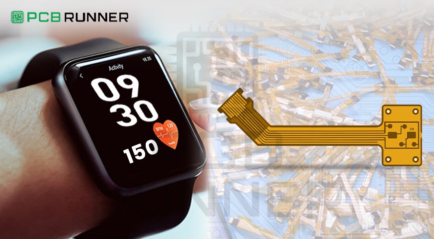
Wearable technology is transforming the way we interact with electronics, from smartwatches and fitness trackers to medical monitoring devices and augmented reality glasses. These devices require Multilayer PCBs that are lightweight, compact, and durable while maintaining excellent electrical performance. The assembly of a Custom Printed Circuit Board for wearables involves specialized techniques to ensure flexibility, reliability, and power efficiency.
As demand for wearable PCB solutions continues to grow, engineers and manufacturers must adopt the best Circuit Board Assembly practices to create high-performance wearable electronic devices. This guide covers essential electronic PCB assembly techniques to improve functionality, durability, and overall performance.
Key Requirements for Wearable PCBs
1. Compact and Lightweight Design
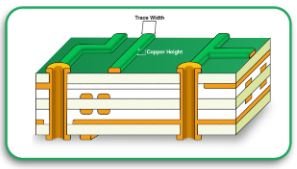
Wearable devices have strict size and weight limitations. PCBs must be thin, flexible, and designed for minimal power consumption. Multilayer PCBs are commonly used to maximize functionality while maintaining a compact footprint.
2. Flexibility and Durability
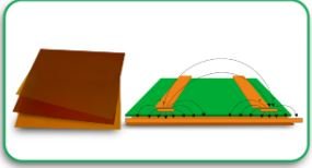
Since wearables experience constant movement, wearable PCBs must withstand bending and flexing without losing functionality. Flexible PCBs or Rigid-Flex PCBs offer improved durability by combining rigid and flexible layers into a single board.
3. Efficient Power Management
Wearable devices operate on small batteries, requiring PCBs with low power consumption. Efficient Circuit Board Assembly ensures minimal energy loss and optimized battery life.
4. Reliable Electronic Component Placement
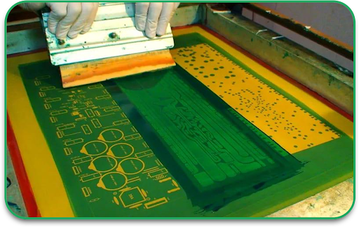
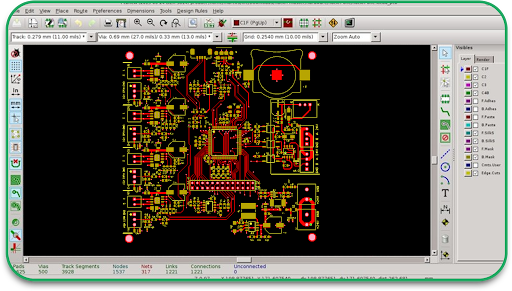
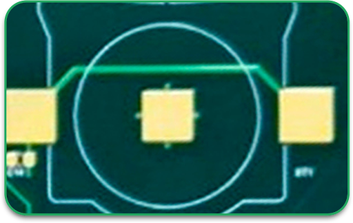
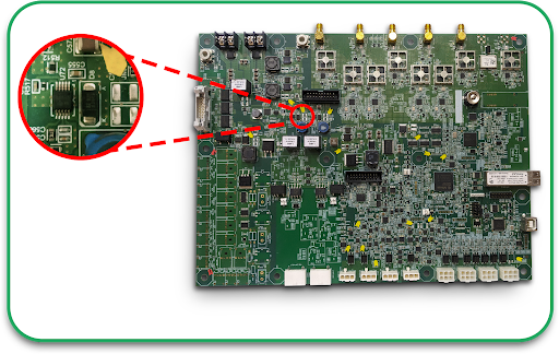
Properly placing and soldering electronic components PCB is critical for the durability of wearable electronics. Using advanced electronic PCB assembly methods like Surface Mount Technology (SMT) improves accuracy and reliability.
PCB Assembly Techniques for Wearable Electronics
1. Using Flexible PCBs
Unlike traditional rigid PCBs, wearable PCB designs often incorporate flexible PCBs to accommodate movement. These boards allow wearable devices to fit comfortably on the body without breaking or losing electrical connectivity.
Advantages of Flexible PCBs:
- Lightweight and space-saving
- Resistant to bending and flexing
- Ideal for compact wearable electronic devices
2. Rigid-Flex PCB Technology
For applications requiring both durability and flexibility, Rigid-Flex PCBs combine stiff and flexible sections into a single Multilayer PCB. These hybrid boards reduce the need for additional connectors and cables, improving reliability.
Benefits of Rigid-Flex PCBs:
- Enhanced structural integrity
- Reduced component failures
- Ideal for fitness trackers and medical wearables
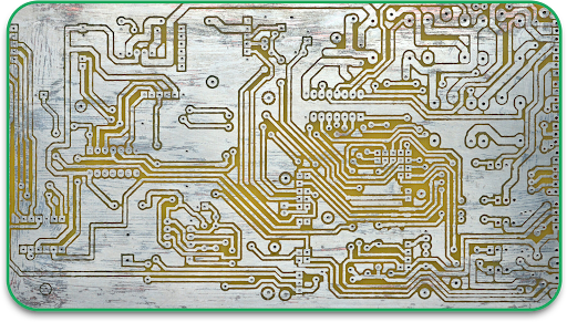
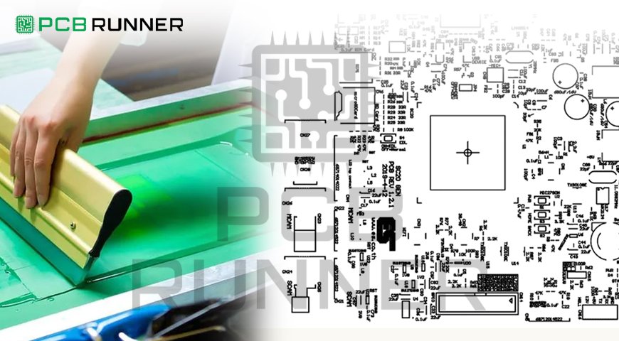
3. Surface Mount Technology (SMT) Assembly
SMT is the preferred method for electronic PCB assembly in wearable electronics. It allows for the placement of miniaturized components directly onto the PCB surface, reducing weight and improving electrical performance.
Why SMT is Ideal for Wearable PCBs:
- Supports high-density component placement
- Improves electrical performance and signal integrity
- Reduces the overall weight of the PCB
4. Low-Power Design Techniques
Since wearables rely on battery power, Custom Printed Circuit Board designs must incorporate low-power consumption techniques.
Power Optimization Methods:
- Use energy-efficient microcontrollers and sensors
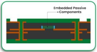
- Optimize power distribution with embedded passive components \
- Implement low-power communication protocols like Bluetooth Low Energy (BLE)
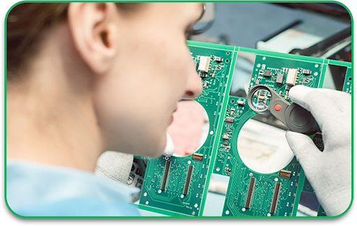
5. Miniaturized Component Placement
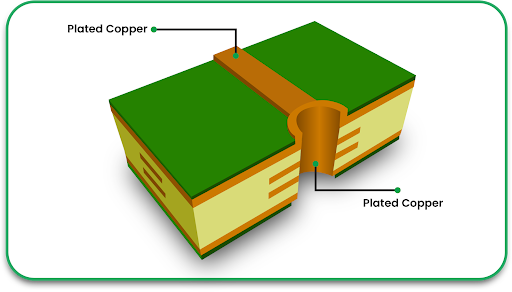
As wearable devices become smaller, PCBs must accommodate electronic components PCB with ultra-fine pitches. High-precision Circuit Board Assembly techniques such as Microvia Technology and High-Density Interconnect (HDI) PCBs enable better performance in compact designs.
Advantages of Miniaturized Components:
- Maximizes space efficiency
- Improves signal transmission speed
- Enhances device aesthetics with slimmer designs
- Material Considerations for Wearable PCB Assembly
Selecting the right materials is crucial for manufacturing durable wearable electronic devices:
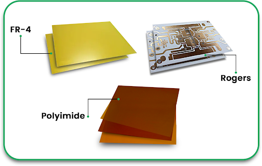
1. Substrate Materials
Wearable PCBs often use polyimide or liquid crystal polymer (LCP) instead of traditional FR-4. These materials provide flexibility, heat resistance, and improved electrical performance.
Common Substrate Choices:
- Polyimide: High flexibility and heat resistance
- LCP: Low moisture absorption and excellent signal integrity
- FR-4: Suitable for rigid sections of hybrid PCBs
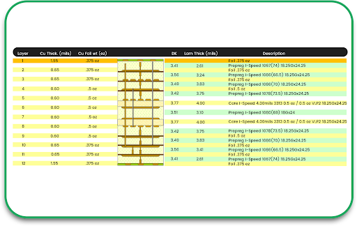
2. Conductive Materials
To ensure optimal electrical performance, wearable PCBs use copper foils with different thickness levels based on current requirements.
Common Conductive Layers:
- Standard copper foils for low-power applications
- Heavy copper PCB layers for power-intensive sections
3. Protective Coatings
Wearable PCBs require protective coatings to safeguard components from sweat, moisture, and physical impact.
Types of Protective Coatings:
- Conformal Coatings: Protect against dust, moisture, and mechanical stress
- Encapsulation (Potting): Provides additional insulation and protection
- Solder Mask Material: Prevents solder bridging and oxidation
Challenges in Wearable PCB Assembly
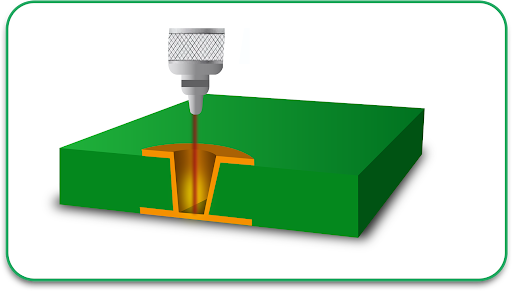
1. Heat Dissipation in Compact Designs
Wearable devices have limited space for heat sinks. PCB manufacturers use thermal vias and graphene-based heat spreaders to dissipate heat efficiently.
2. Component Durability
Since wearables are constantly exposed to motion, electronic components PCB must withstand vibrations and impacts. Using reinforced Circuit Board Assembly techniques helps improve resilience.
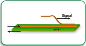
3. Signal Integrity and Interference
High-speed data transmission in wearables requires careful PCB layout design. Shielding techniques and High-Density Interconnect (HDI) PCBs help minimize signal loss and electromagnetic interference (EMI).
Future Trends in Wearable PCB Assembly
1. Stretchable and Biocompatible PCBs
New materials such as stretchable polymers and biocompatible substrates are expanding the possibilities of wearable electronics, particularly in medical applications.
2. Printed Electronics and Flexible Hybrid Electronics (FHE)
Innovations in printed circuit technologies enable cost-effective, lightweight, and customizable wearable PCBs for next-generation smart devices.
3. AI-Driven PCB Assembly Automation
AI-powered electronic PCB assembly is enhancing manufacturing precision, reducing defects, and improving yield rates in high-performance wearable electronics.
Conclusion
High-performance wearable PCB design requires a combination of advanced materials, compact layouts, and precise electronic PCB assembly techniques. By leveraging Multilayer PCBs, Rigid-Flex PCBs, and low-power design methods, manufacturers can create reliable wearable electronic devices that perform well in real-world conditions. For engineers and designers looking to optimize Circuit Board Assembly for wearables, working with experienced PCB manufacturers ensures high-quality fabrication, enhanced durability, and seamless integration of miniaturized components.
Need High-Quality Wearable PCBs?
PCB Runners specializes in Custom Printed Circuit Board solutions for wearable technology. Whether you need Multilayer PCBs, Flex and Rigid PCBs, or specialized Circuit Board Assembly, our expert team is ready to help. Contact us today to discuss your project needs.
Frequently Asked Questions (FAQs)
1. What type of PCB is best for wearable electronics?
Flexible PCBs and Rigid-Flex PCBs are ideal for wearable devices because they allow movement without breaking.
2. Why is low power consumption important in wearable PCBs?
Wearables run on small batteries, so low-power PCB designs extend battery life and improve efficiency.
3. How do you protect wearable PCBs from moisture?
Protective coatings like conformal coatings and encapsulation shield PCBs from sweat and environmental exposure.
4. What is the best soldering method for small wearable PCBs?
Surface Mount Technology (SMT) is preferred for its high precision and ability to handle miniaturized components.
5. Where can I get a custom wearable PCB manufactured?
PCB Runners offers professional wearable PCB manufacturing and assembly services with fast turnaround times. Contact us for a quote today.