If you are looking for better ways to reduce costs and boost performance in your printed circuit board designs, you might have heard about VeCS. This stands for Vertical Conductive Structure. It is a newer method that many engineers are now considering instead of High-Density Interconnect, also known as HDI. HDI has been around for years. It is used in many advanced devices because it can pack a lot of components into a small space. However, HDI can be expensive to make. This is where VeCS comes in. It offers a fresh take on making multilayer printed circuit boards more affordable and efficient.
What Is VeCS and How Does It Work
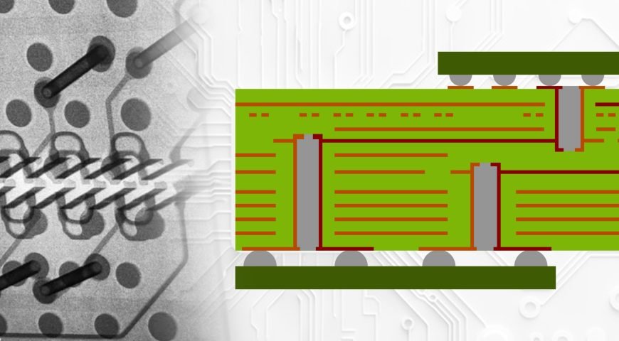
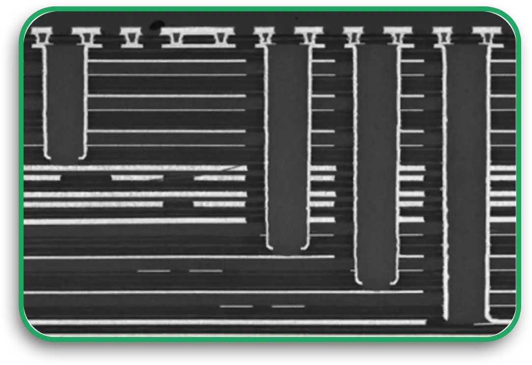
VeCS is a newer method used by printed circuit board manufacturers. Instead of using microvias and stacked vias like HDI, VeCS uses vertical slots or narrow channels to create connections between layers. This is important because microvias used in HDI are hard to make. You need special tools like lasers to drill them. Plus, microvias can only go down one layer at a time. This means you need more steps to build your board. VeCS, on the other hand, uses regular mechanical drilling tools. This makes it easier and cheaper for PCB board manufacturers to work with.
In VeCS, you also do not need as much copper plating. That helps you save time and money in the manufacturing process.
HDI Basics and Why It Costs More
HDI stands for High-Density Interconnect. This technology is used in devices like smartphones, tablets, and wearables. HDI helps you connect many small parts in a small area. It uses micro vias, blind vias, buried vias, and sometimes stacked vias.
Here is the downside. Each of these steps takes time and special tools. For example:
- Microvias need lasers to drill them
- Blind vias only go partway through the board
- Buried vias are hidden inside the board and require multiple steps
These features make HDI PCB boards very powerful, but they also make them costly. If you are making thousands of units, that cost adds up fast.
How VeCS Reduces Costs
VeCS helps reduce costs in many ways. Here are some clear examples:
- Simple Drilling: VeCS uses standard mechanical drills. These are cheaper than laser tools.
- Fewer Steps: Because you do not need to build each layer step-by-step, you save time.
- Less Plating: With VeCS, less copper is needed for plating the holes.
- Lower Scrap Rates: VeCS leads to fewer errors in production, so there is less waste.
All of this means you can get your custom-printed circuit board made faster and cheaper when using VeCS.
How VeCS Improves Efficiency
Cost is not the only benefit. VeCS also helps with signal quality and board performance.
In HDI, stacked vias can sometimes cause signal loss. This happens because each via adds resistance and creates minor electrical problems. When you are working on high-speed designs, this can be a big issue.
VeCS gives you shorter paths and cleaner signals. It also helps with better routing. That means your design will work better in real-life use.
Here is another point: HDI boards often get hotter because they are packed tightly. VeCS boards handle heat better, which helps your devices last longer.
When Should You Choose VeCS
VeCS works best when you need a reliable board but want to avoid the high cost of HDI. This can include products like:
- Industrial controls
- Automotive parts
- Communication systems
- Consumer electronics
If your design does not need ultra-high density like a smartphone, VeCS might be a wise choice.
VeCS also allows you to get more out of your multilayer printed circuit board without jumping into complex and costly HDI methods.
What Printed Circuit Board Manufacturers Think
Many printed circuit board manufacturers are now adding VeCS to their list of services. This is because they see how much it helps their customers save on cost and time. VeCS allows smaller companies to compete with larger ones by offering better prices.
As more PCB board manufacturers adopt VeCS, you can expect better support, more material options, and lower minimum order sizes.
One big bonus is that VeCS is easier to test. HDI boards with micro vias and stacked vias are harder to inspect, making quality control tough. VeCS uses open paths that can be seen and tested with regular tools, which means your boards are more likely to work the first time.
VeCS vs HDI: Key Differences
What to Ask Your PCB Manufacturer
Before choosing between HDI and VeCS, talk to your PCB board manufacturer about your project needs. Ask them:
- Can VeCS support my component layout
- Will I save time and money using VeCS
- Do you have experience with VeCS design
- What is the lead time for VeCS boards
Good printed circuit board manufacturers will help you make the right choice based on your design and budget.
Is VeCS Right for Your Next Project
If you want a better way to manage cost and performance, VeCS is worth investigating. It offers many of the same benefits as HDI but with fewer headaches. You get a strong, reliable, multilayer printed circuit board without paying for complex tools or extra steps. HDI PCB manufacturers still offer great options when your project needs the highest density and smallest size. But for many everyday devices, VeCS offers a better balance of cost and quality. By choosing the right method, you can stay on budget and still meet your performance goals. With more printed circuit board manufacturers supporting VeCS, it is becoming a trusted choice across the industry.
Before you start your next project, compare VeCS and HDI. You might find that VeCS is exactly what you need to build smarter, faster, and more cost-effective electronics.