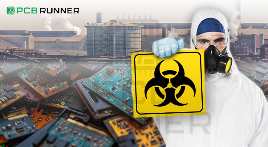
Printed circuit boards, or PCBs, are essential in modern electronics. However, PCB production generates toxic waste that must be managed carefully. If you are involved in PCB fabrication, it is essential to understand how to handle this waste properly. Safe handling protects the environment, ensures compliance with regulations, and keeps workplaces safe.
Understanding Waste in PCB Production
When manufacturing printed circuits, several chemicals and materials contribute to toxic waste. Some of the primary sources include:
- Heavy Metals – Copper, lead, nickel, and other metals are commonly used in PCB production. Improper disposal of these materials can harm water sources and soil.
- Etching Chemicals – The process of removing unwanted copper from PCBs uses strong acids like ferric chloride and ammonium persulfate.
- Soldering Residue – Soldering leaves behind flux and other chemicals that may contain hazardous substances.
- Solvents and Cleaners – Cleaning PCBs involves alcohol, acetone, and other chemicals that can be toxic if released into the environment.
- Plating Solutions – PCB production often involves electroplating, which uses solutions containing cyanide or other harmful chemicals.
Each of these waste types needs proper handling and disposal to reduce their environmental impact.
Steps to Handle Toxic Waste in PCB Manufacturing
1. Identify Hazardous Waste
The first step in handling waste is recognising what is toxic. PCB board production generates different types of waste, including solid, liquid, and gas byproducts. Tracking these materials helps ensure safe disposal.
2. Separate Waste Properly
Not all waste should be mixed together. For example, used etching chemicals should be stored separately from heavy metals. Using dedicated containers for different types of waste prevents dangerous chemical reactions and makes recycling easier.
3. Use Recycling Programs
Many materials used in circuit board production can be recycled. Copper, for instance, is highly reusable. Some PCB circuit board manufacturers partner with recycling facilities to process scrap materials safely. Recycling helps reduce the overall waste produced and lowers the demand for new raw materials.
4. Neutralise Hazardous Chemicals
Some toxic chemicals used in PCB fabrication can be treated before disposal. For example, acids from the etching process can be neutralised with alkaline substances. This reduces their harmful effects on the environment. Some companies use chemical treatment systems to manage waste on-site.
5. Follow Local and International Regulations
Every region has laws governing hazardous waste disposal. Whether you are working with a small PCB manufacturer or a large-scale factory, compliance is necessary. Many countries require permits for handling certain chemicals. Violating these regulations can result in fines and environmental damage.
6. Use Safer Alternatives
Some chemicals used in PCB board production have safer alternatives. For example:
- Lead-free solder reduces the risk of lead contamination.
- Water-based cleaners can replace harmful solvents.
- New etching techniques, such as laser etching, produce less chemical waste.
Switching to eco-friendly materials helps minimise toxic waste while maintaining production quality.
7. Train Employees on Waste Management
Proper training ensures that workers handle hazardous materials safely. Employees should know how to store, transport, and dispose of waste correctly. Regular training sessions help reinforce safe practices and prevent accidents.
8. Invest in Waste Treatment Technology
Many PCB production facilities install waste treatment systems to manage toxic byproducts. Filtration systems can remove heavy metals from wastewater, while air scrubbers reduce harmful emissions. Investing in these technologies improves sustainability in PCB manufacturing.
9. Reduce Waste at the Source
Minimising waste generation is the best way to handle toxic materials. Some methods include:
- Using precise manufacturing techniques to reduce excess material use.
- Implementing closed-loop systems to reuse chemicals.
- Optimising PCB design to require fewer harmful substances.
Benefits of Proper Waste Management in PCB Manufacturing
Handling toxic waste properly benefits both businesses and the environment. Here are some key advantages:
- Protects Natural Resources – Safe disposal methods prevent water and soil contamination.
- Improves Workplace Safety – Reducing exposure to toxic chemicals creates a safer work environment.
- Enhances Company Reputation – Companies that follow environmental regulations gain the trust of customers and partners.
- Reduces Costs – Recycling and waste reduction save money on material purchases and disposal fees.
- Ensures Compliance – Following legal requirements prevents fines and legal issues.
How Manufacturers Can Lead Sustainable PCB Production
As demand for electronics grows, PCB production will continue to expand. Manufacturers must adopt responsible waste management practices to ensure a sustainable future. Some leading companies are already implementing green manufacturing processes, such as using biodegradable materials and energy-efficient production lines.
PCB circuit board manufacturers can also work with suppliers who prioritise sustainability. Choosing environmentally friendly materials and technologies makes a big difference in reducing the industry’s impact on the planet.
Conclusion
Handling toxic waste in PCB manufacturing is a critical part of responsible production. By identifying hazardous materials, following disposal regulations, and using recycling programs, PCB manufacturers can reduce environmental harm. Whether working with multilayer PCB designs or simple circuits, every step toward sustainable waste management improves the safety and efficiency of the industry. If you are involved in PCB production, take action to implement these strategies and contribute to a cleaner, safer future.