


Objective: Give SMT engineers and PCB assembly buyers a technically accurate, practical guide to stencil aperture ratios, thickness selection, and fine-pitch printing, so their first print run comes out clean instead of full of bridging and insufficient paste.
Key Takeaways
- SMT stencil design comes down to two numbers from IPC-7525B: area ratio (minimum 0.66) and aspect ratio (minimum 1.5). Fall below either and the paste starts clinging to the aperture walls instead of releasing onto the pad.
- Stencil aperture ratio problems cause the majority of solder paste printing defects, not the placement machine or the reflow profile. Fix the stencil geometry and most bridging and insufficient-paste issues disappear.
- Laser cut stencil thickness typically runs 0.10mm to 0.20mm. Thinner stencils (0.10-0.12mm) suit fine-pitch QFNs and micro BGAs; thicker ones (0.15-0.20mm) suit connectors and power components.
- Fine pitch stencil printing below 0.4mm pitch needs more than a thinner stencil. Aperture reduction, wall smoothing, and paste type all have to work together.
- Step stencil design solves the problem of one board needing multiple paste volumes, by varying foil thickness across a single stencil instead of forcing a compromise thickness for every component.
A board can have a flawless layout, correctly sized pads, and a well-tuned reflow profile, and still come off the line covered in bridges and cold joints. Nine times out of ten, the fault sits with the stencil, not the process around it.
Industry data consistently points to solder paste printing as the source of most SMT defects, and the stencil is the single biggest variable in that step. Good SMT stencil design isn’t a formality you tick off after layout is done. It’s the difference between paste that releases cleanly onto every pad and paste that clings to the walls and leaves you chasing rework.
This blog walks through the ratios, thickness choices, and stencil types that actually determine print quality, with the numbers pulled from IPC-7525B rather than rules of thumb.
What Is SMT Stencil Design, and How Does It Decide Your Yield?
A stencil is a thin metal sheet, almost always stainless steel, with openings cut to match your board’s solder pads. Get the aperture geometry wrong and no amount of tuning downstream fixes it.
The stencil sits between two fixed points in the process:
- Before it: your PCB layout, pad sizes, and pitch
- After it: placement accuracy and reflow, both of which depend on the paste already being in the right place, in the right volume
Solder paste doesn’t release evenly just because an aperture exists over a pad. It releases based on the ratio between the opening’s area and the surface area of its walls. That ratio, not the aperture size alone, is what IPC-7525B was written to control.
Stencil Aperture Ratio: The Math That Actually Predicts Paste Release
Stencil aperture ratio is calculated two ways, area ratio and aspect ratio, and IPC-7525B sets minimum values for both. Miss either threshold and the paste starts sticking to the walls instead of transferring onto the pad.
Area ratio is aperture opening area divided by aperture wall area:
- For a rectangular aperture: (Length × Width) ÷ [2 × (Length + Width) × Thickness]
- IPC-7525B’s minimum: 0.66
Aspect ratio is the smallest aperture dimension divided by stencil thickness:
- Formula: Width ÷ Thickness
- IPC-7525B’s traditional minimum: 1.5
Below 0.4mm pitch, some fine-pitch designs push aspect ratio down toward 1.0 to 1.2 using electropolished or nano-coated stencils, but that only works with tighter process control. Standard laser-cut stencils should stay above 1.5.
Here’s a quick worked example: a 0.5mm × 0.5mm square aperture cut into a 0.1mm-thick stencil gives an area ratio of (0.25) ÷ [2 × 1.0 × 0.1] = 1.25, comfortably above the 0.66 minimum. Drop that same aperture to 0.3mm × 0.3mm on the same 0.1mm stencil, and the ratio falls to roughly 0.375, well under the threshold, which means that pad is almost guaranteed to print short.
| Ratio | Formula | IPC-7525B Minimum | What Happens Below It |
| Area ratio | Area ÷ (Perimeter × Thickness) | 0.66 | Paste sticks to walls, insufficient deposit |
| Aspect ratio | Width ÷ Thickness | 1.5 | Bridging, incomplete release |
Check both ratios for every aperture, not just the smallest one on the board. A long, narrow aperture can pass aspect ratio and still fail area ratio, so both need verifying independently.
Laser Cut Stencil Thickness: Matching Thickness to Your Smallest Component
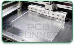
Laser cut stencil thickness is the primary lever for controlling paste volume, and it has to be set by the finest-pitch component on the board, not the average.
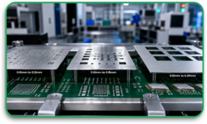
General thickness guidance:
- 0.15mm to 0.20mm: connectors, power components, larger discretes
- 0.10mm to 0.15mm: standard mixed-technology boards
- 0.10mm to 0.12mm: fine-pitch QFNs and micro BGAs
Thicker stencils deposit more paste per aperture. That’s fine for a connector pad, but the same thickness on a 0.4mm-pitch QFN will push the area ratio below 0.66 and cause exactly the sticking problem the ratio math predicts.
The practical rule: let your smallest, tightest-pitch component set the stencil thickness, then adjust aperture size on the larger components to compensate, rather than the other way around. Oversizing apertures slightly on connectors and power parts is a much smaller risk than undersizing a fine-pitch aperture’s ratio.
Fine Pitch Stencil Printing: What Changes Below 0.5mm?
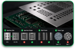
Fine-pitch stencil printing under 0.5mm, and especially under 0.4mm, needs more than a thinner foil. Aperture shape, wall finish, and paste type all start affecting yield in ways they don’t at coarser pitch.
What actually changes at fine pitch:
- Aperture sizing gets tighter. Apertures are typically scaled to roughly 90-95% of the pad dimension to control paste volume without starving the joint.
- Shape matters more. Rounded rectangles and trapezoidal apertures (narrower at the base) release more cleanly than sharp-cornered squares, since corners are where paste tends to hang up.
- Wall finish becomes non-negotiable. Electropolished aperture walls reduce friction during snap-off, which matters far more at 0.3mm pitch than at 0.8mm pitch.
- Paste type has to match. Type 4 or Type 5 paste, with smaller particle sizes, is standard below 0.4mm pitch. Coarser paste particles simply can’t pass cleanly through openings that small.
None of these fixes work in isolation. A thinner stencil with the wrong aperture shape still bridges. The right paste type on a poorly polished stencil still clogs. Fine-pitch printing is a system, and the stencil is only one part of it, though it’s usually the part that gets overlooked first.
Step Stencil Design: When One Thickness Isn’t Enough
Step stencil design solves a problem single-thickness stencils can’t: a board with both fine-pitch ICs and large connectors needs two different paste volumes, and one uniform thickness can’t deliver both correctly.
A step stencil varies foil thickness across the same sheet:
- Step-down areas: thinner material around fine-pitch components, keeping area ratio above 0.66 where it matters most
- Step-up areas: thicker material around large BGAs, edge connectors, or power devices that need more paste volume
There are three common ways fabricators build them:
- Laser-welded: a thicker foil section is cut and welded into a thin base sheet, then apertures are laser cut across the finished, stepped surface
- Etched: the step is formed by chemically etching one side of the foil down to the target thickness in that region
- Micro-machined: a CNC mill cuts the step directly into the stencil material
For a board mixing 0201 passives with a large connector, a step stencil keeps both regions inside their correct ratio range instead of forcing a compromise thickness that under-serves one side and over-pastes the other.
SMT Solder Paste Stencil Types: Laser Cut vs Chemically Etched vs Electroformed
An SMT solder paste stencil can be manufactured three main ways, and the method changes wall quality, cost, and how fine a pitch it can reliably handle.
| Type | How It’s Made | Best For |
| Laser cut | Stainless steel foil cut by precision laser, walls electropolished | Standard through fine-pitch work, most common choice today |
| Chemically etched | Etched from both sides using positive images, leaving an hourglass-shaped wall | Legacy processes, less common now due to less consistent walls |
| Electroformed | Built up layer by layer via electroplating | Ultra-fine pitch, highest cost, smoothest walls |
Laser cutting is the standard choice for the vast majority of boards today, because it produces sharp, consistent aperture edges and gives tighter control over paste volume than the older chemical-etch process, where the hourglass-shaped walls left by double-sided etching make consistent release harder to guarantee.
Getting Stencil Design Right the First Time
A quick pre-order checklist:
- Calculate area ratio and aspect ratio for every aperture, not just the tightest-pitch one
- Set stencil thickness based on your smallest, most demanding component
- Confirm whether a step stencil is needed for mixed fine-pitch and large-component boards
- Specify laser-cut with electropolished walls for anything at or below 0.5mm pitch
- Match paste type (Type 4 or 5 for fine pitch) to your final aperture sizes before ordering
PCB Runner builds laser-cut stencils to match your board’s pad layout as part of the assembly process, so aperture ratios and thickness get checked against your actual components before the stencil is cut, not after the first print run fails.
FAQ
What’s the minimum stencil thickness for fine-pitch components?
Most fine-pitch QFNs and micro BGAs print well on 0.10mm to 0.12mm stencils. Going thinner improves the aperture ratio further but makes the stencil more fragile during handling and printing.
Why does my solder paste keep bridging on small components?
Bridging on fine-pitch parts is almost always an aperture ratio problem, area ratio below 0.66 or aspect ratio below 1.5, not a paste or reflow issue. Recalculate both ratios before adjusting anything else.
Do I need a step stencil for every mixed-component board?
No. If your largest and smallest components don’t differ dramatically in required paste volume, a single well-chosen thickness usually works. Step stencils earn their extra cost when the spread between fine-pitch ICs and large connectors is wide enough that one thickness can’t serve both properly.
Is laser cutting always better than chemical etching for stencils?
For nearly all modern SMT work, yes. Laser cutting gives straighter, more consistent aperture walls than double-sided chemical etching, which matters more as pitch gets finer. Chemical etching still shows up in some legacy or specialty applications.
Does PCB Runner supply stencils alongside PCB assembly?
Yes. PCB Runner provides laser-cut stencils matched to your board’s layout as part of the SMT stencil service, so fabrication and stencil design stay aligned from the start.
Get Your Next Stencil Right the First Time
A well-calculated stencil is the cheapest defect-prevention step in the entire SMT process, and the easiest one to get wrong without the ratio math in front of you.



