


Objective
Electronics are getting smaller, faster, and more complex. Modern printed circuit boards now carry dense components, high-speed signals, tighter spacing, higher power demands, and stricter reliability expectations. Traditional PCB design and manufacturing methods still matter, but they are under more pressure than ever.
In 2026, AI PCB design and manufacturing tools are moving from early experimentation into practical use. Engineering teams are using AI-assisted features for component placement, routing, design checks, signal analysis, thermal review, inspection, sourcing, and process control.
This does not mean AI is replacing engineers. It means engineers now have better tools for repetitive, calculation-heavy, and data-driven work. AI can find patterns faster, compare options quickly, and flag risks earlier. Human engineers are still needed for judgment, trade-offs, product requirements, safety, and final approval.
For OEMs, AI-powered PCB design and smart PCB manufacturing can reduce avoidable errors, shorten development cycles, improve quality control, and support faster time-to-market. PCB Runner works with engineers and OEMs navigating these changes, especially where PCB design, PCB assembly services, PCB manufacturing solutions, and rapid PCB prototyping need to work together.
Key Takeaways
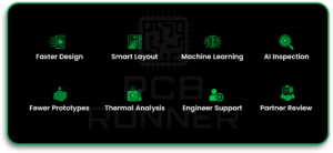
- AI is speeding up PCB design workflows by supporting placement, routing, review, and analysis.
- AI-powered PCB design tools can help reduce repetitive layout work and catch problems earlier.
- Machine learning can support DRC, defect detection, signal checks, sourcing, and process monitoring.
- AI-powered AOI can improve inspection speed and help reduce false calls when trained properly.
- AI can reduce prototype iterations, but it does not remove the need for physical testing.
- AI-assisted thermal and power integrity tools help identify risks before boards are fabricated.
- AI helps engineers, but it does not replace engineering experience or product judgment.
- OEMs should ask PCB partners how they use AI in design review, inspection, sourcing, and quality control.
What Is AI-Powered PCB Design and Manufacturing?
AI-powered PCB design and manufacturing means using artificial intelligence, machine learning, automation, and data analysis to improve how printed circuit boards are designed, checked, built, inspected, and delivered.
In PCB design, AI can support placement, routing, design rule checks, schematic suggestions, signal integrity review, thermal analysis, and power integrity checks. These tools do not design the full product without human input. They help engineers move faster and catch issues earlier.
In PCB manufacturing, AI can support automated optical inspection, defect classification, production monitoring, yield prediction, process drift detection, and component sourcing decisions. This is part of a wider shift toward smart PCB manufacturing.
AI PCB Designer tools are becoming useful because PCB designs now involve more data than one engineer can manually compare quickly. A complex board may include thousands of nets, tight routing rules, multiple voltage rails, dense packages, controlled impedance, RF sections, thermal constraints, and manufacturing limits.
AI helps by reviewing this data quickly and finding patterns that would take much longer to check manually.
How AI Is Transforming PCB Design Workflows
Traditional PCB design can be slow. Engineers manually place components, route traces, check design rules, adjust spacing, review signal paths, and repeat the process until the board is ready.
AI-powered PCB design changes the workflow by helping engineers make better decisions earlier. Instead of waiting until the end of layout to find problems, AI-assisted tools can flag issues while the design is still being built.
For example, an AI-assisted PCB layout tool may suggest better component placement based on signal flow, power paths, heat sources, connector locations, or routing density. It may also identify areas where components are too crowded, traces are likely to become difficult to route, or a layout choice may create manufacturing risk.
This shifts PCB design from a reactive process to a more proactive process. Engineers still make the final decisions, but AI helps reduce wasted time and repeated layout corrections.
For OEMs, this can mean fewer design delays, cleaner PCB layout, better early-stage review, and smoother movement from design to fabrication.
AI-Powered Autorouting: Faster and Smarter Layout Optimization
Autorouting is not new. Traditional autorouters have existed for years, but many engineers avoided them because the results were often messy, inefficient, or difficult to clean up.
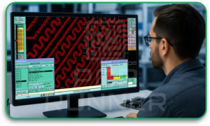
AI-powered autorouting is different because it can use design constraints, routing priorities, learned layout patterns, and optimization methods to suggest cleaner routing paths. It can support trace length control, spacing rules, net priority, impedance requirements, and routing density.
In high-speed boards, routing is not only about connecting one point to another. Trace length, return path, reference plane, via count, coupling, and impedance all matter. AI-assisted routing can help explore routing options faster, especially on dense multilayer PCB designs.
AI autorouting is useful for reducing repetitive work. It can route less critical nets quickly and help engineers focus on high-risk signals, power distribution, RF sections, and sensitive interfaces.
It is still not perfect. Complex mixed-signal boards, RF boards, high-power boards, and safety-critical designs still need experienced engineering review. AI can speed up routing, but it should not be trusted blindly.
Machine Learning for Design Rule Checking (DRC) and Error Prevention
Design Rule Checking, or DRC, checks whether a PCB layout follows required design rules. These rules may include trace width, spacing, via size, clearance, annular ring, solder mask, drill limits, and manufacturer capability.
Traditional DRC is useful, but it is often rule-based. It tells the engineer when a layout violates a defined rule. The problem is that some designs technically pass DRC but still create manufacturing or assembly risk.
Machine learning can improve this process by identifying patterns that have caused problems in past builds. For example, a spacing choice may pass the minimum rule but still be too close to the manufacturer’s practical comfort zone. A footprint may pass the library check but still cause repeat solder defects. A via arrangement may be legal but difficult to fabricate reliably.
AI-assisted DRC can help engineers catch these risks earlier. It can also support real-time feedback during layout instead of only producing a long error list after the board is mostly finished.
For OEMs, this means fewer avoidable revisions, fewer fabrication questions, and fewer late-stage delays.
AI-Driven Signal Integrity and EMI Analysis
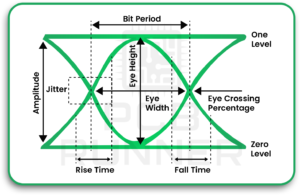
Signal integrity and EMI problems are harder to manage as boards become faster and denser. High-speed digital signals, RF traces, memory interfaces, switching power supplies, and fast clocks can all create noise or performance problems if layout is not controlled carefully.
AI-driven signal integrity tools can help identify areas where reflections, crosstalk, return path breaks, impedance discontinuities, or excessive via transitions may create risk. These tools can support early review before a full simulation setup is completed.
EMI analysis can also benefit from AI. Machine learning models can identify layout patterns that often create radiated or conducted noise. This may include poor ground return paths, noisy switching loops, fast traces near board edges, weak shielding, or poor separation between power and signal sections.
AI does not replace proper SI or EMI engineering. It helps identify risk areas faster, especially during the design stage when changes are easier and cheaper.
For PCB design teams, this can reduce the chance of discovering signal problems only after the prototype fails testing.
Generative AI for Schematic and Layout Suggestions
Generative AI is starting to support early PCB design tasks. It can help suggest common circuit blocks, reference-style schematics, decoupling networks, voltage regulator layouts, connector arrangements, and layout ideas based on known design patterns.
This can be useful for common circuits. A standard power supply section, communication interface, sensor input, or protection circuit can be drafted more quickly with AI support. Engineers can then review, correct, and adapt the suggestion for the real product.
Generative AI can also help document design choices, summarize datasheets, compare component options, or create early design checklists. This can reduce admin work during the early engineering stage.
However, generative AI has clear limits. It can make incorrect assumptions, use the wrong component, miss a constraint, or suggest a circuit that looks reasonable but fails under real conditions. It may also misunderstand safety, compliance, EMC, or manufacturability requirements.
Generative AI should be treated as a support tool, not a final design authority. Every schematic and layout suggestion must be reviewed by a qualified engineer.
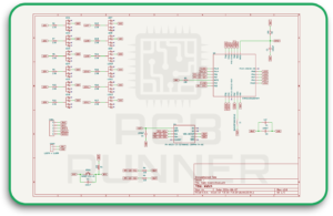
AI in PCB Manufacturing: Automated Optical Inspection (AOI) and Defect Detection
AI is making a strong impact in PCB manufacturing through automated optical inspection and defect detection.
Traditional AOI systems use fixed rules, image comparison, and threshold-based checks. They can detect many common defects, but they may also produce false positives or miss subtle problems. AI-powered AOI uses machine learning and computer vision to improve defect recognition.
AI-enabled AOI can help detect missing components, wrong components, solder bridges, poor solder joints, lifted leads, tombstoning, polarity errors, surface defects, and placement issues. When trained on strong production image data, it can learn the difference between acceptable variation and real defects.
For PCB assemblies, this can reduce manual re-inspection, improve inspection consistency, and help factories find defects earlier.
AI inspection is especially useful in high-volume production where small inspection improvements can save significant time. It also supports smart PCB manufacturing by turning inspection images into useful production data.
AI-based AOI still needs process control and human oversight. The system must be trained, verified, and maintained. Poor training data can create poor inspection results.
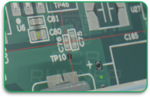
Predictive Quality Control Using AI and Machine Learning
Predictive quality control uses production data to identify problems before they become serious defects.
In PCB manufacturing, machines generate a large amount of process data. This can include solder paste inspection results, placement accuracy, reflow oven profiles, AOI results, X-ray findings, test data, repair logs, and yield reports.
Machine learning can analyze this data and identify patterns. If solder paste volume starts drifting, AI can flag the issue before solder bridges or open joints increase. If placement accuracy changes, the system can warn operators before defects appear across many boards.
This is different from reactive quality control. Reactive quality control finds defects after they happen. Predictive quality control helps identify the process conditions that may cause defects soon.
For OEMs, this can mean more consistent PCB assemblies, fewer surprises during incoming inspection, and better production stability over time.
AI does not remove the need for trained operators, process engineers, or quality teams. It gives them better data to act earlier.
AI in Component Sourcing and Supply Chain Optimization
Component sourcing has become one of the biggest challenges in electronics manufacturing. Shortages, lifecycle changes, counterfeit risk, long lead times, and approved alternate parts can all affect production.
AI can support component sourcing by analyzing stock levels, historical demand, distributor data, lead times, lifecycle status, and basic specifications. It can help identify shortage risks earlier and suggest possible alternate components for engineering review.
For OEMs, this can reduce last-minute sourcing problems. If a microcontroller, power IC, connector, or passive component becomes difficult to source, AI-assisted tools can help find possible options faster.
AI can also support BOM risk review. It can flag obsolete parts, single-source components, non-compliant items, or parts with unstable availability.
However, AI cannot approve substitutes by itself. Alternate parts must be checked by engineers. Footprint, pinout, electrical characteristics, tolerance, voltage rating, thermal rating, firmware compatibility, and compliance must all be reviewed.
AI speeds up sourcing research, but engineering approval remains essential.
How AI Reduces Prototype Iterations and Time-to-Market
Every prototype iteration takes time and money. A board may need a redesign because of routing issues, footprint mistakes, thermal problems, EMI failure, poor power integrity, component availability, or manufacturing defects.
AI can reduce avoidable prototype iterations by catching more issues before fabrication. AI-assisted DFM checks, routing review, signal integrity analysis, thermal review, and BOM risk checks can all help detect problems earlier.
This does not remove the need for rapid PCB prototyping. Physical prototypes are still needed to verify function, assembly, thermal behavior, signal performance, firmware, enclosure fit, and compliance.
The difference is that AI can help the first prototype arrive closer to the intended design. Fewer avoidable errors can mean fewer respins and faster movement from prototype to production.
For OEMs, shorter design loops can improve time-to-market. This matters in competitive industries where product launch timing affects revenue and customer commitments.
AI-Assisted Thermal Management and Power Integrity Analysis
Thermal management and power integrity are becoming more important as boards become smaller and more powerful. Dense components, high-current rails, fast processors, power converters, and compact enclosures can create heat and voltage stability problems.
AI-assisted thermal tools can help identify likely hot spots before the board is built. They can review component power dissipation, copper coverage, airflow, via placement, heat-spreading areas, and mechanical constraints.
AI may suggest changes such as moving heat-generating parts, adding copper pours, increasing thermal vias, adjusting component spacing, or improving heat paths.
Power integrity analysis can also benefit from AI. Tools can help identify weak power distribution areas, voltage drop risks, poor decoupling placement, long return paths, or noisy power zones.
These tools are useful because thermal and power problems can be expensive to fix after assembly. A processor that overheats, a regulator that runs too hot, or a power rail that dips during switching can cause product instability.
AI helps identify risks earlier, but engineers still need to validate the design using proper simulation, datasheets, measurements, and product testing.
Challenges and Limitations of AI in PCB Design and Manufacturing
AI tools are improving quickly, but they are not perfect. They have clear limitations.
The quality of AI output depends on the quality of training data. If a tool is trained on weak, incomplete, or irrelevant data, it may produce poor suggestions. PCB design is also highly context-specific. A layout choice that works in one product may fail in another.
AI can also miss unusual constraints. It may not understand mechanical limits, enclosure effects, compliance requirements, field conditions, customer-specific rules, or safety-related trade-offs unless those details are clearly defined.
Another limitation is integration. Not every AI tool fits smoothly into an existing EDA workflow. Teams may need time to set up libraries, constraints, design rules, manufacturing feedback, and data links.
AI can also create overconfidence. A clean-looking AI-generated result still needs engineering review. A layout may look efficient but have poor return paths, thermal issues, manufacturability risks, or compliance gaps.
AI should be used as a decision-support tool, not a replacement for engineering responsibility.
Will AI Replace PCB Designers and Engineers?
AI will not replace PCB designers and engineers in the near future. It will change how they work.
PCB design requires judgment. Engineers must understand product goals, electrical behavior, manufacturing limits, safety, cost, testing, compliance, reliability, and customer needs. These decisions cannot be fully handed to AI.
AI can handle repetitive work, compare many layout options, flag likely risks, and speed up analysis. It can help with component placement, routing suggestions, design checks, inspection review, and sourcing research.
But engineers still need to decide what matters most. For example, a design may need to balance cost, board size, signal integrity, heat, enclosure shape, test access, component availability, and production yield. AI can support that decision, but it cannot own the final trade-off.
The engineers who benefit most from AI will be the ones who understand both PCB fundamentals and AI-assisted workflows.
The Impact of AI on PCB Manufacturing in the UK and Europe
AI is becoming more important in PCB manufacturing across the UK and Europe because OEMs need better quality, stronger documentation, faster turnaround, and more reliable supply chains.
Many UK and European OEMs serve industries where traceability, compliance, and quality matter. This can include industrial equipment, medical technology, aerospace, automotive, defence, energy, and communication products.
AI can support these needs through smarter inspection, process monitoring, defect tracking, BOM risk review, and production data analysis.
For manufacturers, AI can help improve consistency and reduce avoidable rework. For OEMs, it can provide better visibility into quality and production risks.
AI is also useful because European manufacturers often compete on reliability, engineering support, compliance, and delivery confidence rather than only on the lowest unit price.
As AI adoption grows, OEMs may begin asking suppliers more direct questions about inspection systems, data traceability, process monitoring, and AI-supported quality control.
What OEMs and Engineers Need to Know About AI-Driven PCB Services
OEMs and engineers should understand what AI can and cannot do before choosing AI-driven PCB services.
AI can improve speed, review quality, inspection consistency, and sourcing visibility. It can help reduce avoidable errors and support faster development. But it cannot compensate for poor input files, incomplete BOMs, weak design rules, unclear requirements, or missing engineering review.
When working with a PCB partner, OEMs should ask practical questions. Does the supplier use AI-assisted inspection? How are defects classified? Is AOI supported by human review? Can production data be used to improve yield? Are component sourcing risks flagged early? Can DFM and DFA feedback be provided before fabrication?
Engineers should also keep control of design intent. AI tools work best when constraints are clear. Stack-up, impedance, current requirements, thermal limits, test points, material preferences, compliance needs, and manufacturing rules should be documented properly.
AI-driven PCB services are most useful when they support a strong engineering process, not when they are treated as a shortcut around one.
Conclusion
AI is changing PCB design and manufacturing in practical ways. It is helping engineers work faster, catch risks earlier, improve layout decisions, inspect boards more consistently, and manage supply chain problems with better data.
For PCB design, AI can support placement, routing, DRC, signal integrity, EMI review, thermal planning, power integrity, and schematic suggestions. For manufacturing, AI can support AOI, defect detection, predictive quality control, sourcing review, and production monitoring.
The biggest value is not full automation. The real value is better decision-making earlier in the process.
OEMs and engineers should use AI as part of a stronger PCB development workflow. Clean design data, clear constraints, proper DFM and DFA review, prototype validation, and reliable manufacturing support still matter.
PCB Runner helps OEMs and engineering teams use advanced PCB design technologies, PCB assembly services, PCB manufacturing solutions, and rapid PCB prototyping support to move from concept to production with fewer avoidable delays.
FAQs
Can AI Fully Automate PCB Design?
No. AI can support placement, routing, DRC, analysis, and review, but it cannot fully replace engineering judgment. Complex trade-offs, safety requirements, compliance needs, and unusual design constraints still need experienced engineers.
What Is An AI PCB Designer?
An AI PCB Designer is a tool or platform that uses AI-assisted features to support PCB layout, routing, placement, design checks, schematic suggestions, or analysis. It helps engineers work faster but does not replace final engineering review.
How Does AI Improve PCB Layout?
AI can suggest better component placement, optimize routing paths, flag spacing risks, reduce repetitive layout work, and identify possible signal, thermal, or manufacturability issues earlier in the design process.
How Does AI Improve AOI In PCB Manufacturing?
AI improves AOI by helping inspection systems recognize defects from image data. It can reduce false positives, catch subtle defects, and improve consistency when trained and maintained properly.
Does AI Help With PCB Component Sourcing?
Yes. AI can help review component availability, lifecycle status, lead times, distributor stock, and possible alternates. However, engineers must approve any substitute component before use.
Can AI Reduce PCB Prototype Iterations?
Yes. AI can reduce avoidable prototype iterations by catching DFM issues, routing risks, thermal problems, power integrity concerns, and BOM risks earlier. Physical prototypes are still needed for real validation.
Is AI Useful For Small Engineering Teams?
Yes. AI-assisted PCB tools can help smaller teams access faster checks, layout support, sourcing research, and analysis features. However, the team still needs good design rules, clean libraries, and engineering review.
What Are The Main Limits Of AI In PCB Design?
The main limits are training data quality, incomplete design context, workflow integration, and the need for human judgment. AI can suggest solutions, but engineers must verify them.



