


Get the PCB design wrong, and your AI hardware will fail no matter how good the chip is.
Modern AI processors operate at signal speeds that expose every design flaw. A poorly routed trace, a misplaced decoupling capacitor, or a weak ground plane causes data errors, thermal failures, and EMI problems that no firmware can fix.
PCB Design for AI Hardware is one of the most demanding disciplines in electronics today. Here are 12 rules to get it right.
Objective
To give PCB designers and hardware engineers a clear, accurate, and actionable set of rules for building reliable high-speed AI hardware, covering signal integrity, power delivery, thermal management, and EMI control.
Key Takeaways
- Controlled impedance, differential pair routing, and stackup design are non-negotiable in AI hardware PCB design.
- Power delivery network (PDN) design is just as critical as signal routing
- Via stubs cause signal reflections, back-drilling or blind vias solve the problem
- HDI technology is now standard for high-density AI hardware boards
- EMI, crosstalk, and clock distribution require deliberate design decisions, not afterthoughts
- Early collaboration with your PCB manufacturer prevents costly redesigns
 What Is AI Hardware?
AI hardware is the physical electronic systems built to run artificial intelligence workloads, training neural networks, running inference, or accelerating machine learning.
It includes:
- GPUs – NVIDIA H100, AMD Instinct MI300X, for parallel matrix computation
- TPUs – Google’s custom chips for neural network processing
- NPUs – AI accelerators embedded in edge devices and smartphones
- FPGAs – used in AI inference where low latency and flexibility matter
- AI ASICs – custom silicon for specific tasks like autonomous vehicle perception
All of them generate massive data traffic at very high speeds, consume significant power, and produce significant heat. The PCB has to handle all three, simultaneously.
Why High-Speed PCB Design Is Critical for AI Hardware
Modern AI processors run internal buses at 112 Gbps per lane and above. Memory interfaces like HBM3 and LPDDR5X operate at multi-gigabit rates. PCIe Gen 5 and CXL links leave no room for guesswork.
At these speeds, the PCB is not a passive interconnect. Every trace has impedance, while each via introduces capacitance. Unmatched trace lengths cause timing skew, and gaps in the ground plane create return path problems.
This is why high-speed PCB layout for AI hardware demands strict rules applied consistently, to every single design decision.
Rule 1: Controlled Impedance Traces for High-Speed Signal Integrity
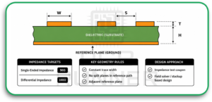
Every high-speed signal must be routed as a controlled impedance trace, typically 50Ω single-ended and 100Ω differential. When impedance is uncontrolled, signals reflect at discontinuities, causing noise and bit errors.
- Calculate trace widths using your stackup and a field solver (Polar Si9000, Saturn PCB Toolkit)
- Maintain consistent trace width, no width changes along a high-speed route.
- Never route high-speed signals over split planes or plane gaps
- Request impedance test coupons from your manufacturer to verify after fabrication
Rule 2: Minimising Trace Length for Critical High-Speed Signals
Shorter traces mean less attenuation, less delay, and less interference. At 56 Gbps and above, even a few extra millimetres of trace causes measurable signal degradation.
- Place processors, memory, and high-speed devices as close together as possible
- Use length matching within differential pairs and across bus lanes tolerance is typically ±5 mil or tighter.
- Avoid 90° corners use 45° angles or curved routing
- Eliminate unnecessary stubs
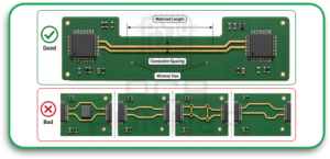
Rule 3: Proper Differential Pair Routing for SerDes and Data Buses
PCIe Gen 5, USB4, 112G Ethernet, and HBM memory all use differential signalling. It only works when pairs are routed correctly.
- Keep both traces of a pair tightly coupled with spacing per your impedance target.
- Match lengths within the pair to ±1 mil for the fastest interfaces
- Never split a pair around an obstacle
- Maintain consistent spacing throughout the route
- Minimise vias in differential pair routes; every via adds capacitance and can upset balance.e
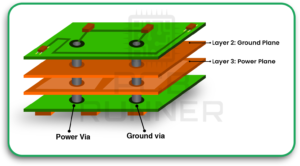
Rule 4: Power Plane and Ground Plane Management for Low Noise
A solid, continuous ground plane is the single most important element of a well-designed signal integrity PCB. It provides a low-impedance return path for every signal on the board.
- Every signal layer needs a reference plane (ground or power) directly adjacent to .it
- Never route high-speed signals over a split plane, return current detours around gaps, creating loop antennas.
- Use plane stitching vias near high-frequency components and board edges
- Keep power planes close to their adjacent ground plane to reduce PDN inductance
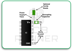
Rule 5: Decoupling Capacitor Placement for AI Processors
AI processors switch billions of transistors per second. Each switching event draws a sharp current spike. Without local decoupling, that spike causes voltage droops that destabilise the processor.
- Place decoupling capacitors within 0.5 mm of the component power pins
- Use multiple values in parallel 100 nF and 10 nF, to cover a wide frequency range
- Use low-ESL X5R or X7R MLCC capacitors
- For BGA packages, place capacitors in the via field under the package not just around the perimeter
- Combine bulk capacitance (10–100 µF) with high-frequency bypass (100 nF, 10 nF)
PDN simulation using tools like Ansys SIwave or Cadence Sigrity is strongly recommended for AI processor boards.
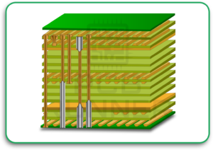
Rule 6: Via Management Minimising Via Stubs and Using Back-Drilling
Every through-hole via has a stub the unused barrel below the signal layer. At high frequencies, this stub resonates and reflects signal energy back into the trace. Above 10 Gbps, via stubs is a serious problem.
- Back-drilling: A second controlled-depth drilling operation removes the stub. Cost-effective for backplane and high-layer-count designs.
- Blind vias: Laser-drilled vias that only reach the required layer no stub formed at all. Cleaner but more expensive.
- Via-in-pad with copper fill: Places the via directly under the BGA pad for the shortest possible signal path.
Keep via count on high-speed traces to a minimum. Each via adds approximately 0.5–1 pF of capacitance.
Rule 7: Stackup Design for Multi-Layer High-Speed PCBs
The stackup is the foundation of your entire high-speed PCB layout. Every impedance calculation and reference plane assignment depends on it.
- Place a reference plane adjacent to every signal layer
- Bury high-speed signal layers between reference planes to reduce radiation
- Use symmetrical construction about the board centre to prevent bow and twist
- For designs above 10 GHz, use low-loss laminates Rogers, Megtron 6, or Megtron 7 instead of standard FR-4
- Specify copper weight per layer 0.5 oz on inner layers allows finer trace widths for impedance control
Stackup planning must happen before routing begins not after.
Rule 8: Avoiding Crosstalk Through Proper Trace Spacing
Crosstalk is noise induced on one trace by a neighbouring trace. At high signal speeds, even closely spaced traces couple enough energy to cause bit errors.
- Apply the 3W rule; maintain spacing of at least 3× the trace width between high-speed signals.
- Route high-speed traces on layers with adjacent ground planes to contain fields
- Alternate routing direction between layers; horizontal on one layer, vertical on the next
- Keep aggressor signals (clocks, high-swing outputs) away from sensitive receivers.
Crosstalk is a geometry problem. Fix it in the layout.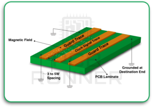
Rule 9: Handling Clock Signal Routing and Clock Tree Distribution
Clocks drive processors, memory, SerDes, and FPGAs simultaneously. Poor clock routing causes jitter, setup/hold violations, and system instability.
- Route clocks in a dedicated layer or isolated routing channel
- Treat every clock trace as a controlled impedance trace; 50Ω single-ended or 100Ω differential
- Usea star topology or an H-tree distribution to deliver equal propagation delay to multiple loads
- Add series termination resistors (22–33Ω) at the source to reduce reflections
- Avoid vias mid-route on clock traces; each via adds stub and capacitance
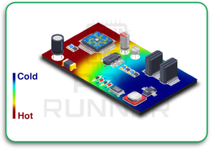
Rule 10: Thermal Management for High-Power AI Chips
The NVIDIA H100 has a TDP of 700W. Even edge AI chips dissipate tens of watts in a small area. Without proper thermal design, solder joints crack and components fail.
- Use thermal via arrays under high-power components; 0.3 mm diameter, 0.6 mm pitch is a common starting point.
- Fill thermal vias with copper or thermally conductive epoxy for maximum conductivit.y
- Use copper pours on exposed layers to spread heat laterally
- For extreme power density, consider embedded copper coins directly under the component
- Place high-power components near the board edge or heatsink mounting points
- Run thermal simulation (ANSYS Icepak, FloTHERM) before manufacturing
Rule 11: EMI Control; Shielding, Filtering, and Board-Level Grounding
High-speed AI boards generate significant electromagnetic emissions. Without deliberate control, boards fail FCC, CE, or CISPR certification.
- Maintain a complete, uninterrupted ground plane; gaps force return currents to loop and radiate.
- Add ferrite beads or LC filters on all I/O lines and cables, leaving the board.
- Use guard rings around clock circuits and oscillators
- Add edge stitching vias along the board perimeter, spaced at less than λ/20 of the highest frequency
- Decouple every power entry point with bulk and high-frequency capacitors before the internal PDN
Rule 12: Design for Testability (DFT) in High-Speed AI PCB Assemblies
A board that cannot be tested reliably cannot be manufactured reliably.
- Add test point pads (minimum 1 mm diameter) on power rails, clocks, reset lines, and the key data bus
- Implement JTAG boundary scan (IEEE 1149.1) on all compliant processors and FPGAs
- Use built-in loopback test ports on SerDes interfaces for bit error rate testing (BERT)
- Ensure every power rail has a test point accessible to automated test equipment.
- Use the BIST (Built-In Self-Test) features of AI processors during board bring-up and production test.
HDI PCBs and Their Role in AI Hardware Design
HDI is no longer optional for AI hardware. AI processors with 2000+ ball BGA packages simply cannot be routed on standard multilayer boards.
HDI enables:
- Micro vias (50–150 µm) for fine-pitch BGA fanout
- Via-in-pad for the shortest signal path under BGA packages
- Stacked and staggered vias for dense multilayer interconnects
- ELIC (Every Layer Interconnect) for the highest routing density
Combining HDI with advanced PCB technologies low-loss laminates, back-drilled vias, embedded components gives you the full toolkit for demanding AI hardware designs.
Common High-Speed PCB Design Mistakes in AI Hardware
| Mistake | Consequence | Fix |
| Routing over plane gaps | EMI, signal degradation | Continuous reference plane under all high-speed traces |
| Mismatched differential pairs | Timing skew, noise | Length-match within ±1 mil |
| No PDN simulation | Voltage droop under load | Simulate PDN, add decoupling |
| Via stubs on 56 Gbps signals | Eye closure, reflections | Back-drill or use blind vias |
| No thermal path under AI chips | Thermal failure | Thermal vias, copper pour, heatsink |
| No test points on critical nets | Untestable boards | Add 1 mm test pads on all key nets |
Most of these share one root cause high-speed design decisions made too late. Stackup, plane structure, and component placement must be resolved before routing starts.
Working With Your PCB Manufacturer Early
Bring your manufacturer in before you start routing. Early engagement gives you:
- Stackup validation based on their actual material capabilities
- DFM feedback on micro via sizes, back-drill tolerances, and annular ring minimums
- Material availability confirmation for Rogers, Megtron 6, or PTFE laminates
- Impedance coupon placement for meaningful post-fabrication verification
- Realistic lead times for complex HDI, back-drilled, controlled-impedance boards
Using modern PCB design techniques alongside a manufacturer who understands high-speed requirements is how reliable AI hardware gets built on the first spin.
At PCB Runner, we support high-speed AI hardware designs from stackup planning through fabrication with DFM review, controlled impedance verification, and IPC Class 3 capability.
Conclusion
AI hardware performance is ultimately limited by the PCB it runs on. The fastest processors cannot compensate for a poor board design.
These 12 rules — applied consistently, simulated before manufacturing, and validated with your fabrication partner — are the baseline for serious PCB Design for AI Hardware in 2026.
Stay current with the latest PCB design trends as AI hardware continues to push the limits of what a printed circuit board can do.
PCB Runner works with AI hardware teams who need technical depth, fast turnaround, and a manufacturing partner who understands what high-speed design actually demands. In high-speed AI hardware design, there are no small decisions. Every trace, every via, and every plane choice either helps your signal or hurts it.
Working on an AI hardware board? Share your Gerber files with PCB Runner and get a technical DFM review before you commit to fabrication.
FAQs
What impedance should high-speed traces on AI hardware PCBs target?
Single-ended signals target 50Ω. Differential pairs typically target 100Ω, though PCIe Gen 5 specifies 85Ω differential for the channel. Always check the interface specification and processor reference design for the correct target.
What laminate should I use for PCIe Gen 5 or 56 Gbps designs?
Standard FR-4 is not suitable above 10–15 Gbps over long traces. Use low-loss laminates Panasonic Megtron 6, Isola I-Speed, or Taconic RF-35. For mmWave applications, Rogers RO4003C or PTFE-based laminates are appropriate.
How close should decoupling capacitors be to an AI processor?
Within 0.5 mm of the power pins. For fine-pitch BGAs, place capacitors in the via field under the package not only around the perimeter. The goal is to minimise inductance in the power delivery loop.
What is the difference between back-drilling and blind vias?
Back-drilling mechanically removes the stub from an existing through-hole via. It is cost-effective for thick, high-layer-count boards. Blind vias are laser-drilled only to the required depth — no stub is ever created. Blind vias provide cleaner signal integrity. However, they also increase manufacturing cost and complexity.
How many layers does a typical AI hardware PCB need?
Most AI hardware boards run 12 to 20 layers. High-end server and data centre boards can reach 24 or more. Layer count is driven by BGA routing density, the number of power rails, and the need for dedicated reference planes on every signal layer.



