


AI is not coming to PCB engineering. It is already here – and it is changing how boards are designed, built, and tested.
From automated routing to real-time solder inspection, AI-based electronics manufacturing is moving fast. The question is no longer whether AI belongs in PCB engineering. It is how to use it well – and where it still falls short.
Key Takeaways
- AI is being applied across the entire PCB design and assembly value chain
- Automated routing, DRC checking, and signal integrity analysis are already AI-assisted in leading EDA platforms
- AI-driven inspection and process monitoring are reducing defect rates in SMT assembly
- Data quality, legacy tool integration, and infrastructure cost remain real barriers
- AI supports engineers; it does not replace them
- Choosing an AI-ready manufacturing partner matters more than ever in 2026
Introduction: The Intersection of AI and PCB Engineering
PCB engineering has always been detail-heavy. A single board can have thousands of components, hundreds of nets, and dozens of constraints that must all be satisfied at once. Getting it right manually takes time, experience, and careful review at every stage.
AI changes the speed and scale at which that work gets done. Machine learning models evaluate thousands of routing options in seconds. Computer vision systems catch solder defects faster than human inspectors. Predictive algorithms flag equipment faults before they cause production rejects.
This is not about replacing expertise. It is about applying it more efficiently and catching mistakes that even experienced engineers miss under time pressure.
The PCB manufacturing process is one of the most process-intensive operations in electronics. Every stage of design, fabrication, assembly, and test generates data. AI turns that data into actionable intelligence.
How AI Is Being Applied Across the PCB Value Chain
AI is not one tool. It is a set of techniques in machine learning, computer vision, and generative design applied at different points in the PCB workflow.
Here is where it is active today:
- Design: Automated routing, DRC, signal and power integrity analysis, generative layout suggestions
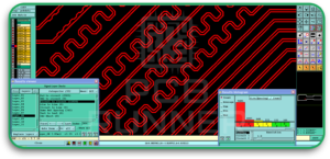
- Fabrication: Process parameter optimisation, yield prediction, defect detection in panel imaging
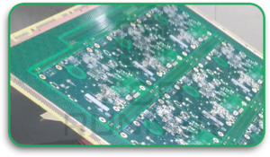
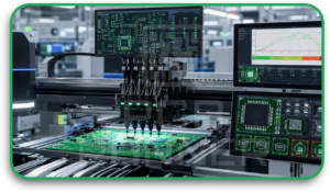
- Assembly: Solder paste inspection, pick-and-place optimisation, reflow profile tuning, AOI classification
- Test: Intelligent fault diagnosis, anomaly detection in functional test data
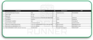
- Supply chain: Component availability prediction, BOM risk analysis, alternate part recommendations
Each application is at a different level of maturity. Some are standard in production today. Others are still emerging.
Benefits of AI in PCB Design
Faster Design Iterations
Traditional PCB layout is iterative and slow. A designer routes the board, runs a DRC, finds violations, fixes them, and repeats. For complex multilayer HDI designs, this takes days or weeks.
AI-assisted tools like Cadence Allegro X AI and Altium’s AI routing engine can complete routing for entire signal groups in minutes. This removes the rule-mechanical work so engineers focus on decisions that require real judgement.
Automated Layout and Routing Optimisation
Generative design AI proposes component placement options based on signal flow, thermal constraints, and keepout zones simultaneously. This is especially valuable in automated circuit board production, where optimised placement reduces routing complexity, layer count, board area, and cost.
Improved Signal and Power Integrity
AI-based tools now embed signal integrity checking directly into the routing environment. They flag impedance mismatches, return path problems, and differential pair violations in real time as the designer works, not after.
Power integrity analysis, PDN simulation, decoupling adequacy, and voltage droop estimation are similarly being integrated into AI-assisted design flows. Catching these issues during layout saves significant time compared to finding them at board bring-up.
Reduced Human Error in DRC
AI-enhanced DRC goes beyond geometric rule checking. It identifies patterns associated with manufacturability problems trace-to-via clearances that are technically legal but likely to cause yield issues, silkscreen overlapping pads, or copper features difficult to etch at the specified line width. This is a layer of intelligence that standard rule-based DRC simply does not have.
Benefits of AI in PCB Assembly
AI-Enhanced Solder Paste Inspection
Solder paste inspection (SPI) is one of the highest-value steps in SMT assembly. Too much paste causes bridging. Too little causes weak joints or openings. Traditional SPI uses fixed rule-based thresholds. AI-based SPI systems learn from production data, adapt to process drift, and classify marginal deposits more accurately, reducing both false rejects and missed defects.
Smarter Pick-and-Place Machine Programming
Programming a pick-and-place machine for a new design involves defining feeders, nozzle assignments, pick sequences, and placement order. Optimising this manually takes hours. AI algorithms generate placement programs that minimise head travel, balance feeder usage, and reduce cycle time automatically. Some systems improve their own programs over successive production runs.
Real-Time Process Monitoring and Adjustment
Reflow soldering is sensitive to oven temperature profiles, conveyor speed, and atmospheric conditions. AI-driven process monitoring tracks these variables in real time and makes closed-loop adjustments without waiting for an engineer to review a trend chart. This is the core of AI-driven manufacturing solutions, moving from reactive quality control to proactive process control.
Predictive Maintenance for Assembly Equipment
Unplanned downtime on an SMT line is expensive. AI predictive maintenance systems monitor motor currents, vibration signatures, nozzle accuracy, and feeder performance. They identify degradation before failure and schedule maintenance during planned stops. Companies using predictive maintenance report 20–40% reductions in unplanned downtime.
AI Applications in PCB Quality Control and Testing
AI transforms AOI from a rule checker into a learning system. AI-based AOI trained on large defect image libraries can:
- Distinguish genuine defects from false alarms with higher accuracy
- Classify defect types: bridging, insufficient solder, missing component, tombstoning automatically
- Flag systematic defects that point to a process problem rather than a random failure
- Reduce false call rates, which are one of the biggest productivity losses in SMT assembly
- In functional and flying probe testing, AI prioritises test sequences based on failure likelihood, focusing test time on nets and components most likely to fail based on historical data.
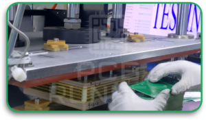
X-ray inspection for BGAs and stacked via structures also benefits from AI image classification, evaluating solder void percentage and joint shape far more consistently than manual review.
AI in Component Sourcing and BOM Management
The global component shortage of 2020–2022 exposed how fragile manual BOM management is. AI is now applied practically to sourcing:
Availability prediction: ML models trained on distributor inventory and lead time data flag at-risk components before they go on allocation
Alternate part identification: AI analyses datasheets and cross-references specifications to propose qualified alternates, cutting hours of manual review
BOM risk scoring: AI scores entire BOMs for supply chain risk, single-source parts, end-of-life status, geopolitical exposure
Price trend analysis: Predictive models help procurement teams time purchases to avoid price spikes
For high-mix, low-volume manufacturers common in European PCB manufacturing and assembly services, AI-assisted BOM management reduces time and risk on complex assemblies.
Real-World Applications in Automotive, Medical, and Defence
Automotive: ADAS and EV battery management systems demand boards that operate reliably across extreme temperatures and 15+ year lifespans. AI is used in design validation to simulate failure modes and in assembly to enforce the process controls required for IATF 16949 compliance.
Medical: AI-assisted design tools help medical device manufacturers meet IPC Class 3 and ISO 13485 requirements by embedding compliance checking into the design flow. AI-driven traceability systems log every process parameter for every board, essential for FDA and MDR audits.
Defence: Defence PCBs operate in high-vibration, high-temperature environments with zero tolerance for field failure. AI simulation tools predict mechanical stress, thermal fatigue, and vibration-induced solder joint failure before the first prototype is built.
Challenges of Implementing AI in PCB Design and Manufacturing
Data Quality and Training Requirements
AI models are only as good as the data they are trained on. A manufacturer with inconsistent process records, incomplete defect logs, or poorly labelled AOI images will not get good results. Building a clean, labelled, consistent process data infrastructure is a significant upfront investment that many operations underestimate.
Integration with Legacy EDA Tools
Many PCB design teams use workflows that have been in place for years. AI features in newer platforms do not always integrate cleanly with legacy tools, file formats, or PDM systems. Migration carries real risk and cost, especially for teams with large libraries of existing designs.
Cost and Infrastructure Barriers
Enterprise AI platforms are expensive. For small and mid-size PCB manufacturers, the capital cost of AI-enabled inspection systems and process analytics tools is difficult to justify without clear ROI data. Cloud-based AI tools are lowering this barrier, but meaningful gaps remain for smaller operations.
AI and IPC Compliance: Ensuring Standards Are Met Automatically
IPC-A-610 and IPC-A-600 define acceptability criteria for assembled and bare boards. Applying these standards consistently across shifts, operators, and product types has always been a challenge.
AI-based inspection systems trained directly on IPC acceptability criteria make classification decisions to accept, reject, or review against a consistent standard rather than relying on individual inspector interpretation. For Class 3 work in medical and defence, this consistency is not just a quality benefit. It is an audit requirement.
Will AI Replace PCB Designers and Manufacturing Engineers?
No, but it will change what they spend time on.
Routine, rule-mechanical tasks, basic routing, standard DRC, repetitive inspection classification are being automated. What remains requires contextual judgement, system-level thinking, and creative problem-solving. These are things AI does not do well.
Engineers who thrive in an AI-assisted environment are those who can direct AI tools effectively, validate outputs critically, and know when to override them.
The Future of AI-Driven PCB Manufacturing in the UK and Europe
European manufacturers are investing in AI to compete on quality and responsiveness. Key trends shaping the near future:
- Digital twins of assembly lines, AI models that mirror the real process and allow virtual optimisation before physical trials
- Closed-loop process control equipment that adjusts its own parameters in real time based on inspection feedback
- AI-assisted DFM manufacturer-side tools that automatically review customer design files against production capabilities before fabrication
Regulatory pressure – RoHS, REACH, MDR, and IEC standards are also driving AI adoption as compliance documentation and traceability requirements grow more demanding.
How to Work With an AI-Ready PCB Manufacturer
Not all manufacturers are at the same level of AI adoption. When evaluating a partner for your next PCB assembly project, ask:
- Do they use AI-based AOI and SPI on their SMT lines?
- Can they provide real-time process data and full traceability records?
- Do they offer AI-assisted DFM review as part of quoting?
- Are inspection classifications traceable to IPC-A-610 criteria?
For your PCB design work, check whether your EDA platform has AI-assisted routing, real-time SI checking, and intelligent DRC features enabled.
At PCB Runner, we work with design teams and OEMs who need a manufacturing partner that understands modern design flows, supports thorough DFM review, and maintains the process discipline that AI-driven quality systems depend on.
Conclusion
AI is not a future consideration for PCB design and assembly; it is active in how leading manufacturers and design teams operate today.
The benefits are real: faster design cycles, fewer defects, better process control, and more consistent quality. So are the challenges: data infrastructure, legacy integration, and adoption cost for smaller operations.
The manufacturers and engineers who navigate this shift well adopt AI tools thoughtfully, understanding what they do reliably, where they need human oversight, and how to fit them into workflows that already work.
PCB Runner is committed to supporting that shift with the process capability and manufacturing discipline that AI-driven quality depends on.
“AI makes good PCB engineering faster. It does not make poor engineering good. The fundamentals still matter most.”
Planning your next PCB design and assembly project? Talk to PCB Runner about DFM review and assembly capabilities that support your timeline and quality requirements.
FAQs
1. Is AI-assisted PCB routing reliable enough for production designs?
For standard and moderately complex boards, yes. AI routing tools in Altium and Cadence produce DRC-clean results efficiently. For high-speed, HDI, or mixed-signal designs, AI routing works best as a starting point that an experienced engineer reviews and refines. It handles the mechanical work the engineer handles the signal integrity judgement.
2. How does AI improve AOI accuracy in SMT assembly?
Traditional AOI uses fixed thresholds. AI-based AOI learns from thousands of labelled images and classifies joints probabilistically. This reduces false calls on good joints and improves detection of genuine defects, particularly subtle ones like insufficient solder or marginal component placement, more consistently than rule-based systems.
3. What data does an AI-driven SMT process monitoring system need?
Consistent, timestamped process data, oven temperature profiles, SPI measurements, placement accuracy logs, and AOI results linked to individual board serial numbers. The richer and more consistent the historical data, the more accurately AI can identify process drift and predict failure modes.
4.Can AI help with component shortages and BOM risk?
Yes. AI tools trained on distributor inventory, lead time history, and component lifecycle data flag at-risk parts early and suggest qualified alternates. This is particularly useful for long-lifecycle products in medical, defence, and industrial markets where obsolescence is a genuine design concern.
5. Does AI in PCB manufacturing affect IPC certification requirements?
AI does not change IPC standards. IPC-A-610 and IPC-A-600 acceptability criteria remain the same. What AI changes is how consistently those criteria are applied. AI inspection systems trained on IPC criteria deliver more repeatable classification than manual inspection, supporting compliance rather than undermining it.



