



Objective
To give engineers, designers, and procurement teams a technically accurate and easy-to-follow guide to how PCBs are made, what materials and standards are involved, and how to choose the right manufacturing partner.
Key Takeaways
- The PCB fabrication process involves multiple tightly controlled steps, and each one affects board quality.
- Material selection directly impacts electrical, thermal, and mechanical performance.e
- Surface finishes like ENIG, ENEPIG, and Hard Gold serve very different purposes.s
- HDI technology uses blind, buried, stacked, and staggered vias to enable denser designs
- IPC-A-600, IPC-A-610, ISO 9001, ISO 13485, and ISO 14001 are key quality benchmarks
- Prototyping and production require different approaches and priorities
- RoHS and REACH compliance is now a baseline requirement for European markets
 The PCB Manufacturing Process: Step-by-Step
The PCB manufacturing process is a sequence of precise, interdependent steps. A mistake at any stage can cause the entire board to fail.
Design and Gerber File Preparation
Everything starts with the PCB design. Engineers use tools like Altium Designer, KiCad, or Eagle to lay out traces, pads, vias, and copper pours. Once the design is complete, it is exported as Gerber RS-274X files, the standard format manufacturers use to produce the board.
A complete file package includes:
- Gerber files for every copper layer
- Excellon drill file (hole locations, sizes, plated vs non-plated)
- Fabrication drawing with stack-up, tolerances, and special notes
- Silkscreen, solder mask, and board outline layers
Always run a Design Rule Check (DRC) before submitting. Errors caught at this stage cost nothing to fix. Errors caught after manufacturing cost everything.
Material Selection
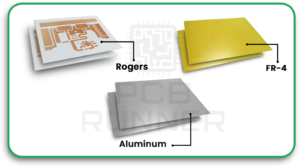
The base laminate is chosen based on the application. FR-4 for general-purpose designs. Rogers or PTFE for high-frequency. Aluminum for thermal management. Ceramic for extreme environments. More on materials in Section 4.
Imaging and Etching
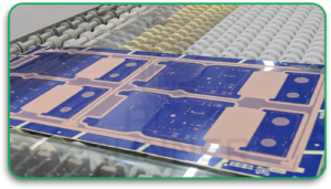
The copper-clad laminate is coated with a dry film photoresist. A photomask representing the circuit pattern is placed over the board and exposed to UV light. The exposed areas harden. The unexposed areas wash away. Chemical etching then removes the unwanted copper, leaving only the defined traces and pads.
Layer Lamination
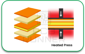
For multilayer boards, individual inner layers are stacked with prepreg (pre-impregnated glass-fibre resin sheets) between them. The stack is bonded under heat and pressure. Alignment between layers, called registration, must be extremely precise. Even a small misregistration can cause opens or shorts between inner layers.
 Drilling
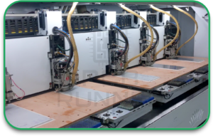
Through-holes are drilled using high-speed CNC machines. Micro vias for HDI designs are created using laser drilling. CO₂ or UV lasers can produce holes as small as 50–75 microns, which mechanical drills simply cannot achieve.
Plating
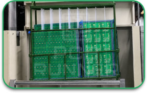
After drilling, holes are plated with copper using an electroless copper process, followed by electrolytic plating. This creates the electrical connection between layers through the via barrel.
Solder Mask and Silkscreen
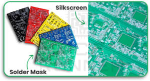
The solder mask, usually green, though other colours are available, is applied over the copper traces. It prevents solder bridges during assembly and protects copper from oxidation. The silkscreen layer adds component reference designators, polarity marks, and logos.
 Final Inspection and Testing
Every board goes through:
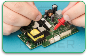
- Automated Optical Inspection (AOI) checks trace integrity, pad conditions, and solder mask coverage
- Electrical testing, flying probe (no fixture needed) or bed-of-nails (faster for volume), verifies all nets
- X-ray inspection used for buried vias, stacked micro vias, and BGA pads
 Types of PCBs: Rigid, Flex, Rigid-Flex
Rigid PCBs use a solid FR-4 or similar substrate. They are the most common type and suit most applications.
Flex PCBs use polyimide (PI) substrate. They bend and fold without breaking. Common in wearables, cameras, and compact medical devices.
Rigid-flex PCBs combine rigid and flexible sections on a single board. They eliminate connectors, reduce weight, and improve mechanical reliability, but they cost more to design and manufacture.
Types of Critical PCBs
HDI (High-Density Interconnect)
HDI boards use micro vias, fine lines, and sequential lamination to pack more circuitry into less space. Used in smartphones, tablets, and high-performance computing.
Burn-In Boards
Purpose-built for reliability testing. Components are stressed under elevated temperature and voltage to identify early-life failures. These boards must survive hundreds of thermal cycles.
ELIC (Every Layer Interconnect)
ELIC is the most advanced interconnect technology available today. Copper-filled stacked microvias connect each layer to adjacent layers. The design eliminates skip layers, enables the highest possible routing density, and powers the latest flagship smartphones and advanced chip packaging technologies.
Core Constructions
Manufacturers build traditional multilayer boards around a central core and add build-up layers to both sides. Designers use coreless constructions in advanced IC substrates and packages when applications require superior symmetry, thinner profiles, and enhanced signal performance.
PCB Materials in 2026
| Material | Best Application | Key Property |
| FR-4 | General purpose | Cost-effective, good mechanical strength |
| Rogers (RO4003C, RO4350B) | RF, microwave, 5G | Low Dk, low Df, thermally stable |
| Aluminum | LED, power electronics | High thermal conductivity |
| Ceramic | Aerospace, high-temp | Excellent thermal and electrical stability |
| Low-loss PTFE | mmWave, satellite, defense | Extremely low dielectric loss at high frequency |
FR-4 remains the standard for digital and mixed-signal designs. It is cost-effective and well-understood.
Rogers laminates offer a tightly controlled dielectric constant (Dk) and very low dissipation factor (Df). This matters in radar, antenna design, and anything above 5 GHz.
Aluminum PCBs bond a copper circuit layer to an aluminum base through a dielectric. Heat generated by LEDs or power components transfers directly into the aluminum and dissipates.
Low-loss PTFE is used where signal loss at millimeter-wave frequencies cannot be tolerated, such as in 5G infrastructure, satellite communication, and defense radar systems.
Copper Thickness, Trace Width, and How They Affect Performance
Copper weight is measured in ounces per square foot (oz/ft²). Standard is 1 oz (35 µm). Heavy copper boards use 2 oz, 3 oz, or higher typically for power electronics and busbars.
Trace width must be calculated, not guessed. A trace that is too narrow for its current load will heat up, increase resistance, and eventually fail. Key factors:
- Current (amperes)
- Copper weight (oz/ft²)
- Allowable temperature rise (°C)
- Internal vs external layer location
The IPC-2221 standard provides the reference formulas and tables for trace width calculations.
Spacing between traces defines voltage isolation. It also controls crosstalk in high-speed designs. For high-voltage boards, creepage and clearance distances must comply with IEC 60950 or IEC 62368.
Fine trace and space, such as 3 mil / 3 mil or tighter,r requires HDI-level imaging and etching processes. Standard PCB fabrication processes typically hold 4–5 mil minimum.
Surface Finish Options
The surface finish protects exposed copper pads and ensures good solderability. Choice affects shelf life, assembly process, cost, and long-term reliability.
| Finish | Key Feature | Best For |
| Lead-Free HASL | RoHS-compliant, slightly uneven surface | General through-hole and larger SMT |
| ENIG | Flat, solderable, 12+ month shelf life | Fine-pitch SMT, general assembly |
| ENEPIG | Nickel + palladium + gold, no black pad risk | Mixed assembly, wire bonding |
| OSP | Organic coating, flat surface, short shelf life | Low-cost SMT, fast-turn production |
| Immersion Silver | Flat, good solderability | High-speed signal boards |
| Immersion Tin | Flat, suits press-fit connectors | Backplane, connector boards |
| Hard Gold (30–70µ”) | Thick electroplated gold, wear-resistant | Edge connectors, sliding contacts |
| Soft Gold (up to 10µ”) | Pure, pliable gold | Wire bonding, low insertion-force contacts |
ENIG is the most widely used finish for modern SMT assembly. It is flat, reliable, and has a long shelf life.
ENEPIG adds an electroless palladium layer between the nickel and gold. This eliminates the black pad defect, a corrosion failure mode in ENIG, caused by hyper-corrosion of the nickel during gold deposition. ENEPIG supports both soldering and wire bonding on the same board.
Hard Gold at 30µ” to 70µ” thickness is used on card edge connectors and contacts that experience repeated insertion cycles. It is highly wear-resistant but expensive.
Soft Gold up to 10µ” is used in wire bonding. The gold must be pure and soft enough for the ultrasonic bonding process to form a reliable weld.
Laser Drill Micro Vias and HDI Technology
HDI technology allows more connections in less space. It uses micro vias, sequential lamination, and fine lines to achieve routing densities impossible with standard multilayer construction.
Via Types in HDI
Blind Via:
Connects an outer layer to one or more inner layers. Does not pass through the full board thickness. Can be laser-drilled or mechanically drilled.
Buried Via:
Connects inner layers only. It is not visible from either outer surface. Must be drilled and plated before outer layers are laminated.
Stacked Vias:
Micro vias placed directly on top of each other across consecutive layers. Gives the densest interconnect. Requires copper filling and planarisation at each lamination step to ensure the next via has a solid landing pad.
Staggered Vias:
Micro vias offset between layers rather than stacked. Easier to manufacture reliably. Less dense than stacked but more dependable.
ELIC (Every Layer Interconnect):
Stacked copper-filled micro vias on every layer, outer to inner and back. No layer is bypassed. Maximum signal routing density. Used in the most advanced portable electronics and packaging substrates.
Laser drilling uses CO₂ lasers for dielectric-only vias and UV (Nd: YAG) lasers for direct laser vias through copper foil. UV lasers are more precise and are used for finer hole sizes.
Importance of IPC Standards and ISO Certifications
Quality is not visible. Manufacturers build quality through disciplined processes and verify compliance with international standards.
IPC-A-600: Acceptability of Printed Boards
IPC-A-600 defines what is acceptable and what is not on a bare PCB. It covers:
- Conductor integrity (cracks, voids, nicks, pinholes)
- Laminate condition (delamination, measling, blistering, crazing)
- Hole and via quality (barrel cracks, nodules, voids in plating)
- Surface conditions (scratches, stains, exposed copper)
Three acceptance classes:
- Class 1 – General electronics, lowest reliability requirement
- Class 2 – Dedicated service electronics (most commercial products)
- Class 3 – High-reliability: military, aerospace, life-critical medical
IPC-A-610: Acceptability of Electronic Assemblies
IPC-A-610 is the world’s most widely used standard for assembled PCBs. It covers solder joint quality (SMT and through-hole), component placement and orientation, cleanliness, and conformal coating. The same three-class system applies.
ISO Certifications
ISO 9001 – Quality Management System. Documents processes, enforces corrective actions, and requires regular audits. This is the minimum baseline for any serious manufacturer.
ISO 13485 – Medical Device QMS. Adds risk management, design controls, and product traceability requirements specific to medical-grade manufacturing.
ISO 14001 – Environmental Management System. Governs how a manufacturer handles chemical waste, water discharge, energy use, and emissions. Increasingly required in European supply chains.
Always verify certifications directly. Ask for the certificate number and check it against the issuing body’s registry.
PCB Prototyping vs Production: Key Differences
| Factor | Prototyping | Production |
| Quantity | 1–50 boards | 100s to millions |
| Lead time | 24 hours – 5 days | 2–6 weeks |
| Cost per board | Higher | Lower |
| DFM check | Basic | Full review |
| Testing | Sample | 100% electrical |
| Panelisation | Often, a single design | Step-and-repeat panels |
For prototypes, speed is the priority. You want to verify and iterate quickly. For production, yield, consistency, and unit cost matter most.
Panelisation is often overlooked at the prototype stage. In production, boards are manufactured as a PCB Panel, with multiple individual boards grouped on a single manufacturing panel. The panel format (V-score, tab-route, or combined) affects assembly efficiency, yield, and cost.
Moving from prototype to production is the right time to do a full DFM (Design for Manufacturability) review. Design decisions that are harmless at low volume can cause serious yield issues at scale.
Environmental Compliance: RoHS, REACH, and Sustainable Manufacturing
RoHS (Restriction of Hazardous Substances) prohibits lead, mercury, cadmium, hexavalent chromium, and certain brominated flame retardants in electronic equipment sold in the EU.
REACH (Registration, Evaluation, Authorisation and Restriction of Chemicals) governs chemical substances used in manufacturing, including Substances of Very High Concern (SVHCs). Manufacturers must track and disclose these through the supply chain.
Beyond compliance, responsible manufacturers are:
- Recovering and recycling copper from process waste
- Reducing water consumption in wet chemical processes
- Switching to water-soluble flux systems
- Measuring and reporting carbon footprint
If your product targets the European market,s especially in medical, automotive, or consumer electronics, full RoHS and REACH documentation from your manufacturer is non-negotiable.
How to Prepare Your Files for PCB Manufacturing
Incomplete or incorrect files are one of the most common causes of manufacturing delays.
Minimum file package:
- Gerber RS-274X files: top and bottom copper, all inner copper layers, top and bottom solder mask, top and bottom silkscreen, board outline (mechanical layer)
- Excellon drill file: plated and non-plated holes, correct units (metric or imperial)
- Fabrication drawing: board dimensions, stack-up, copper weight, surface finish, controlled impedance specs, any special requirements
For complex designs, also include:
- Stack-up specification with dielectric thickness and material callouts
- Controlled impedance requirements with target Ω values and reference layers
- IPC-2581 or ODB++ files as alternatives that bundle everything in one package
Common errors to avoid:
- Missing inner layer files
- Drill file units mismatch (metric vs imperial)
- Solder mask openings not matching pad sizes
- No controlled impedance callout on sensitive signal layers
- Incorrect board outline or missing cutouts
Confirm file format requirements and layer naming conventions with your manufacturer before submitting.
Common PCB Manufacturing Defects and How They Are Prevented
| Defect | Root Cause | Prevention |
| Open circuit | Broken trace, over-etching | AOI, DFM review, etch process control |
| Short circuit | Solder bridge, under-etching | Correct trace spacing, AOI |
| Delamination | Moisture in the laminate, incorrect cure | Humidity-controlled storage, process control |
| Barrel crack in via | Thermal stress, poor copper plating | Correct aspect ratio, controlled plating thickness |
| Black pad (ENIG) | Nickel corrosion under the gold layer | Use ENEPIG, control plating bath chemistry |
| Measling/crazing | Internal laminate stress, moisture | Correct lamination temperature and pressure |
| Bow and twist | Uneven copper distribution, incorrect stackup | Balanced copper pour, correct stacking symmetry |
| Via void | Poor electroless copper coverage | Process chemistry control, pre-clean steps |
AOI catches most surface-level defects. X-ray inspection finds hidden issues in buried vias, stacked micro vias, and BGA solder joints. Flying probe testing gives 100% electrical coverage with no fixture, practical for prototypes and low-volume runs. Bed-of-nails testing is faster for high-volume production, where a dedicated fixture cost is justified.
Choosing a Reliable PCB Manufacturer in Europe and the UK
Supply chain disruptions have pushed many companies to source PCBs closer to home. European manufacturers offer shorter lead times, easier communication, and stronger compliance alignment.
Key Factors to evaluate:
- Certifications: ISO 9001 minimum. ISO 13485 for medical. ISO 14001 for environmental compliance. ITAR registration for defense.
- Technical capability: Can they handle HDI, controlled impedance, heavy copper, flex, or rigid-flex? Or only standard rigid boards?
- Traceability: Full material and process traceability is essential for medical, automotive, and aerospace supply chains.
- DFM support: A manufacturer who reviews your files and flags issues before production saves you time and money.
- Lead time: European manufacturers typically deliver standard boards in 5–10 working days. Fast-track options of 24–48 hours exist for urgent prototypes.
- Communication: Response speed and technical transparency matter. You want a partner who explains problems, not one who just rejects files.
At PCB Runner, we combine technical capability with fast turnaround and full compliance support from first prototype to production ramp.
Before going to manufacture, review your PCB Design thoroughly. Many costly manufacturing problems originate in the design stage and are entirely avoidable with the right review process.
Conclusion: Getting the Most from Your PCB Manufacturing Partner
The PCB fabrication process in 2026 demands more precision, more compliance, and more technical alignment between designer and manufacturer than ever before. Boards are smaller, faster, and operate in harsher environments, and they still have to work the first time.
By understanding how manufacturers produce circuit boards, you can make better design decisions, create clearer specifications, and ask the right questions before production begins. It turns a transactional supplier relationship into a real technical partnership.
PCB Runner is here to support that partnership from file review and DFM feedback to fast-turn prototyping and full production runs.
Precision starts at the design stage and is verified at every step of manufacturing. Partner with people who take both seriously.”
Ready to start your next project? Submit your Gerber files and get a quote today.
FAQs
What is the typical lead time for PCB manufacturing?
Standard prototype lead times range from 24 hours to 5 working days. Complex multilayer, HDI, or special-material boards take longer. Production quantities typically require 2–6 weeks, depending on complexity and volume. Always confirm lead time based on your specific design and stack-up.
What is the difference between ENIG and ENEPIG?
ENIG deposits electroless nickel, then immersion gold. ENEPIG adds an electroless palladium layer between them. The palladium acts as a barrier that prevents nickel corrosion during gold deposition,n eliminating the black pad defect. ENEPIG also supports wire bonding alongside soldering, making it suitable for mixed-process assemblies.
How many layers does a PCB typically have?
Most boards have 2 to 8 layers. Simple consumer products often use 2 or 4 layers. High-complexity designs in smartphones, servers, and aerospace systems can reach 16, 24, or more layers. Layer count is driven by routing density, signal integrity, and power distribution requirements.
What is a PCB Panel and why does it matter?
A PCB Panel is a larger manufacturing panel that contains multiple individual boards grouped together. Panels allow boards to travel efficiently through SMT assembly lines. Panel design, including tooling holes, fiducials, and breakaway method (V-score or tab-route), directly affects assembly yield and cost. Standard panel dimensions and design guidelines are covered in detaHDI boardsil at PCB Runner’s panel guide.
What is the minimum file set needed for PCB fabrication?
At minimum: Gerber RS-274X files for all layers, an Excellon drill file, and a fabrication drawing. For controlled impedance designs, also include a stack-up specification and impedance targets. ODB++ or IPC-2581 is accepted by most modern manufacturers as a complete alternative to individual Gerber files.



