
Get your PCB dimensions wrong, and your board will not run on the assembly line, no matter how well the circuit is designed.
Designers spend weeks on schematics, routing, and component selection. Then they submit a board that does not fit the manufacturer’s panel properly, is too wide for a standard EU conveyor, or has components sitting right at the edge clearance zone. These are not complex problems. They are avoidable ones. Understanding PCB manufacturer size limits before layout begins saves redesign time, avoids production delays, and significantly reduces costs.
PCB Runner works with engineering teams across Europe on exactly these issues. This guide covers everything you need to know about PCB dimensions for EU assembly, clearly and with real numbers.
Key Takeaways
- PCB size directly affects panel utilisation, fabrication cost, and assembly compatibility
- EU assembly lines have specific conveyor width and board dimension requirements
- Most manufacturers work within a maximum panel size of 457mm x 610mm
- Edge clearance, fiducial placement, and board thickness all have defined dimensional requirements
- Confirming dimensions with your manufacturer before layout saves costly respins

Why PCB Dimensions Matter for EU Assembly
Dimension errors cause real production problems. A board that is too wide for a conveyor cannot run through automated assembly without manual handling, which adds cost and slows everything down. Components placed too close to the edge are vulnerable to damage during depaneling. Poor panel utilisation can also increase expenses significantly, as wasting 40% of a fabrication panel may effectively double the unit cost before any other factor comes into play.
EU electronics manufacturing follows IPC-2221 as the primary design standard, alongside EN 61188 for printed board assemblies. These define acceptable dimensional ranges for boards going through automated SMT lines. Understanding these ranges before you start laying out the board is far more efficient than finding problems after files are submitted.
Every dimension decision connects to something downstream. Board size affects panel yield. Panel yield affects cost. Board width affects conveyor compatibility. Conveyor compatibility affects whether your board can be assembled automatically at all. None of this is complicated once you know the numbers, but ignoring it can lead to expensive surprises.
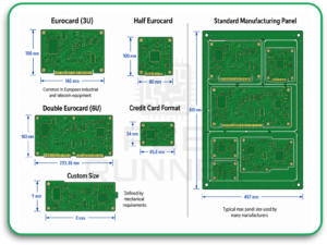
Standard PCB Sizes Used in European Manufacturing
There is no single mandatory PCB size. Your mechanical requirements and component count determine your board size. But certain size formats are considered standard in European production, which simplifies panel utilisation and reduces fabrication costs.
Commonly used PCB formats in EU manufacturing:
- Eurocard (3U): 100mm x 160mm, the most widely used format in European industrial and telecom equipment
- Half Eurocard: 100mm x 80mm, compact industrial applications
- Double Eurocard (6U): 233.35mm x 160mm, rack-mounted systems
- Credit card format: 85.6mm x 54mm, embedded modules and smart card applications
- Custom sizes: defined entirely by product mechanical requirements
The Eurocard format is particularly significant for EU manufacturers because it aligns with standard 19-inch rack systems used throughout European industrial electronics. Designing to Eurocard dimensions when your application allows it simplifies integration and often improves panel utilisation.
EU Assembly Line Dimension Requirements
European SMT assembly lines running IPC Class 2 and Class 3 production have specific conveyor and handling constraints. The most commonly used assembly platforms in European contract manufacturing, Fuji NXT, Panasonic NPM, JUKI FX series, share similar dimensional working ranges.
Standard EU SMT assembly line constraints:
| Parameter | Minimum | Maximum |
| Board width (conveyor direction) | 50mm | 460mm |
| Board length | 50mm | 610mm |
| Board thickness | 0.4mm | 4.0mm |
| Component-free edge zone | 3mm | 5mm |
| Depaneling clearance | 1mm | — |
Boards narrower than 50mm cannot run through standard conveyors without a carrier frame or panel extension. Boards wider than 460mm require special handling or must be split into sections. Both situations add cost and complexity that a small design adjustment during layout could have avoided entirely.
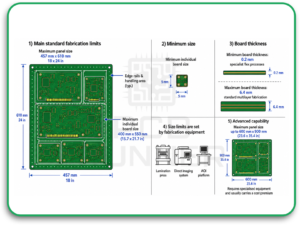
PCB Manufacturer Size Limits
PCB manufacturer size limits are set by the physical dimensions of fabrication equipment, specifically the lamination press, direct imaging system, and AOI platform.
Standard fabrication size limits at most manufacturers:
- Maximum panel size: 457mm x 610mm (18″ x 24″)
- Maximum individual board size: approximately 400mm x 550mm, the remaining margin is used for panel edge rails and handling
- Minimum individual board size: 5mm x 5mm for standard processes
- Maximum board thickness: 6.4mm for standard multilayer fabrication
- Minimum board thickness: 0.2mm for specialist flex processes
Some advanced PCB manufacturers can handle larger panels up to 600mm x 900mm, but this requires specialised equipment and carries a cost premium. It also narrows your options significantly when qualifying backup suppliers.
Always request your specific manufacturer’s capability datasheet before finalising board outline dimensions. Published capability ranges sometimes differ between standard and premium pricing tiers at the same facility.
PCB Panel Sizes and Cost Impact
Fabricators charge per panel, not per individual board. The number of your pcb boards that fit on a standard panel directly determines your unit fabrication cost. This is one of the most impactful and most overlooked cost factors in PCB design.
A standard 457mm x 610mm pcb panel size has a usable fabrication area of approximately 420mm x 570mm after edge rails are removed.
Panel yield comparison example:
This is why a small change in board dimensions during layout, sometimes as little as 5 to 10mm in one direction, can meaningfully improve panel yield and reduce unit fabrication cost. This analysis should happen before the layout is complete, not after.
Minimum PCB Size Constraints
Very small boards create handling problems in automated production. Any board below 50mm in either dimension needs special consideration for EU assembly.
Common solutions for small boards:
- Panel arrays, multiple copies of the small board connected as a single larger panel that runs through the line normally, then separated after assembly
- Carrier frames, rigid frames that hold small boards at a manageable size during assembly, and are removed afterward.
- Tab-routed panels, boards connected by perforated breakaway tabs within a larger panel structure
The minimum fabricable size in standard processes is 5mm x 5mm. For boards below 50mm x 50mm, always confirm handling capability with your assembly provider before finalising the board outline. Finding out during production that your board needs a custom carrier adds lead time and cost that could have been planned for from the start.
Edge Clearance and Keep-Out Zones
Every PCB needs a component-free zone around its perimeter. This zone serves three purposes: conveyor rail support, panel handling during fabrication, and clearance for depaneling operations.
EU standard edge clearance requirements:
- Conveyor edge (long edge of board): minimum 3mm, recommended 5mm
- Remaining edges: minimum 2mm, recommended 3mm
- Via-free zone from board outline: minimum 1mm
- Copper-free zone from board outline: minimum 0.3mm for standard fabrication
Placing components inside the conveyor edge clearance zone is one of the most common causes of assembly damage. The conveyor rail physically contacts the board edge during transport through the SMT line. Anything in that zone is at risk of mechanical damage during processing.
Fiducial Marker Placement Rules
Fiducial markers are copper reference points used by pick-and-place machines to align the board during automated assembly. They are mandatory for any board undergoing automated SMT production.
Fiducial requirements for EU SMT assembly:
- Minimum three fiducials per board for full X-Y-theta alignment
- Fiducial diameter: 1mm copper circle
- Solder mask clearance around fiducial: 3mm minimum
- Placement location: board corners, within component area but outside edge keep-out zone
- Minimum distance from board edge: 5mm
For fine-pitch components, anything with a lead pitch below 0.5mm, including BGAs and fine-pitch QFPs, local fiducials placed directly adjacent to the component significantly improve placement accuracy. These are in addition to the global board fiducials, not a replacement for them.
Board Thickness Standards
Board thickness affects conveyor handling, component support during reflow, and the mechanical rigidity of the finished assembly.
Standard thickness options and applications:
Thickness: Typical Application
0.8mm Compact modules, usually require a carrier in standard EU lines
1.0mm Thin consumer devices, wearables
1.6mm Universal standard, compatible with all EU assembly lines
2.0mm Industrial equipment requiring additional rigidity
2.4mm High-power boards with heavy components
3.2mm Structural or bus bar applications
1.6mm is the right choice unless your design has a specific mechanical reason to deviate. It is compatible with every standard EU assembly line, supported by every fabricator, and creates no handling complications. Non-standard thicknesses narrow your supplier options and can affect pricing at multiple manufacturers simultaneously.
Panelization Methods for EU Production
Panelization groups individual boards onto a manufacturing panel for efficient fabrication and assembly. The separation method chosen affects component placement rules near board edges.
Three main methods used in EU production:
V-score (V-groove): A V-shaped groove is cut along separation lines. Boards snap apart after assembly. Requires straight, parallel separation lines. Minimum distance from V-score line to nearest component: 1mm. Produces a slightly rough edge after separation.
Tab routing with breakaway tabs: Boards are held in the panel by small perforated tabs, typically 0.5mm drill holes in a row. Allows non-rectangular board shapes. Tabs are broken or routed after assembly. Requires clearance around each tab location for the routing tool.
Full routing with edge rails: Boards are fully separated from panel material, held only by the panel rails. Produces the cleanest board edge. Used when edge finish quality is critical. Creates more material waste than the V-score.
The panelization method needs to be agreed with your assembly provider before the layout is finished, because each method has different implications for where components can be placed near the board outline.
Common Dimension Mistakes That Cause Production Problems
These are the errors that come up most consistently in submitted designs:
- The board is too wide for a standard conveyor, requires manual handling or a carrier frame, both of which add cost.
- Components placed inside the edge clearance zone, damaged by conveyor rails or depaneling tooling
- No fiducials on the board, automated placement cannot be set up without them
- Board thickness not confirmed with assembler, causes conveyor jamming or requires an unplanned carrier.
- Panel utilisation was not analysed before layout, board dimensions waste 40 to 50 percent of the panel area unnecessarily.
- Depaneling clearance not maintained, routing tool damages nearby components during panel separation
- Non-rectangular board outline with no tab-route plan, requires custom tooling that adds cost and lead time.
Every one of these is avoidable. Every one of them is caught easily during a dimensional review before files are finalised.
Conclusion
PCB dimensions are a core design parameter, not background details to sort out at the end.
Board size determines panel yield and fabrication cost. Width determines conveyor compatibility. Thickness determines assembly line handling. Edge clearance determines whether components survive depaneling. Fiducial placement determines whether automated assembly can even begin. All of these need deliberate decisions made early in the design process, with your manufacturer’s actual capabilities confirmed before layout is locked.
PCB Runner supports EU engineering teams from the earliest design stage, reviewing board dimensions, confirming panel utilisation, and identifying assembly constraints before they become production problems.
Dimension your board for the factory, not just the product. Get it right before layout, and everything downstream moves faster and costs less.
FAQs
What Is the Maximum PCB Size for Standard EU Assembly Lines?
Standard EU SMT assembly lines handle boards up to 460mm wide and 610mm long. The maximum fabrication panel size at most manufacturers is 457mm x 610mm (18″ x 24″). Individual board size is typically limited to around 400mm x 550mm to allow for panel edge rails and handling margins.
What Happens If My PCB Is Too Small for Automated Assembly?
Boards below 50mm in either dimension cannot run through standard EU conveyors unassisted. They require panel arrays, carrier frames, or tab-routed panels to handle them in automated production. Always confirm handling capability with your assembly provider for boards measuring less than 50mm x 50mm.
How Does PCB Size Affect Fabrication Cost?
PCB size affects cost through panel utilisation. Fabricators charge per panel. Boards that yield fewer copies per panel have proportionally higher unit cost. A board that is 15mm wider than necessary might reduce panel yield by 30 percent, increasing unit fabrication cost by a similar amount.
What Edge Clearance Is Required for EU PCB Assembly?
EU SMT assembly requires a minimum 3mm component-free zone along conveyor edges and a 2mm zone along the remaining edges. A 5mm clearance on all sides is recommended for any board going through standard automated production. Components placed inside these zones risk damage during conveyor transport and depaneling.
Is 1.6mm always the Right Board Thickness?
For most applications, yes. 1.6mm is compatible with all standard EU assembly lines, supported by every fabricator, and creates no handling complications. Thinner boards below 0.8mm or thicker boards above 3.2mm require explicit capability confirmation from both your fabricator and your assembly provider, significantly narrowing your manufacturing options.

