
Small design decisions made early can either save you thousands in production or cost you far more than necessary, and most engineers only find out which after the boards come back.
The truth is, most PCB cost problems are not manufacturing problems. They are design problems. Industry data consistently shows that up to 80% of a product’s total manufacturing cost is locked in during the design phase. PCB design optimization is the most direct lever you have for controlling what you spend, and it costs nothing to get right at the start compared to what it costs to fix later.
PCB Runner works with design teams across industries, and the pattern is consistent, boards that come in over budget almost always have design choices that could have been avoided with a bit of planning. This guide covers every major area where smart design decisions reduce manufacturing cost without compromising what your board needs to do.
Key Takeaways
- PCB manufacturing cost is mostly decided during the design stage, not after the board reaches production.
- Layer count, board size, material choice, via type, component count, and surface finish all have a direct impact on final cost.
- Using standard materials like FR-4 can reduce cost when the application does not require advanced laminates.
- Fewer layers can lower cost, but only when signal integrity, power delivery, and performance are still protected.
- Simple layouts, consistent trace widths, standard drill sizes, and proper spacing make boards easier and cheaper to manufacture.
- Good panelization reduces material waste and lowers the cost per board, especially in higher-volume production.
- Standard components and fewer unique parts can reduce assembly time, feeder setup, sourcing issues, and inspection complexity.
- Blind and buried vias should only be used when needed because they add extra fabrication steps and cost.
- DFM review helps catch design issues early, improves first-pass yield, and reduces rework, scrap, and production delays.
- The cheapest PCB design is not always the best design. The goal is to balance performance, reliability, manufacturability, and cost from the start.
Why PCB Design Has a Direct Impact on Manufacturing Cost
Design Decisions That Increase or Reduce Cost
Every choice you make during PCB design, how many layers, what material, how many vias, which components, directly affects fabrication and assembly cost. These are not abstract decisions. They translate into real production steps, real materials, and real labor time. A four-layer board does not cost twice as much to produce as a two-layer board. It costs roughly three to four times more, because lamination, drilling, and registration all increase non-linearly with layer count.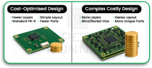
Relationship Between Design Complexity and Production Expense
Complex designs require more process steps, tighter tolerances, more inspection, and higher scrap risk. All of those things cost money. A design that is more complex than it needs to be is not just wasteful, it actively increases the risk of yield loss and rework, which adds cost beyond the base fabrication price.
Importance of Cost Planning at the Design Stage
Cost planning needs to happen in parallel with electrical and mechanical design, not after layout is complete. By the time a designer has finished routing a 12-layer board with blind vias and an ENIG finish, most of those cost decisions are locked in. Revisiting them means significant rework. Starting with cost in mind costs nothing.
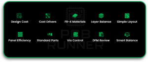
Understanding the Key Cost Drivers in PCB Manufacturing
The major cost factors in PCB manufacturing are well understood. Here they are, ranked by typical impact:
Number of Layers and Board Complexity
Every layer adds lamination cycles, registration requirements, and processing time. A 2-layer board is the cheapest. A 4-layer board costs roughly 30–50% more. An 8-layer board can cost two to three times as much as a 4-layer board. Layer count is your biggest single lever for controlling PCB material costs.
Board Size and Panel Utilization
PCBs are fabricated on panels, typically 18″ x 24″. Your board size determines how many copies fit on one panel. A board that wastes 40% of the panel area is effectively paying for material it does not use. Designing your board size with panel utilisation in mind is one of the simplest and most overlooked cost-optimisation opportunities.
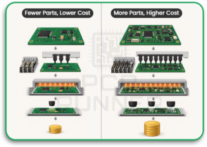
Assembly Complexity and Component Count
More components mean more placement operations, more soldering, more inspection, and more opportunity for error. Each unique component also requires a separate feeder on the pick-and-place machine, which adds to the setup cost. Reducing the component count and standardising component types reduces assembly costs proportionally.
PCB Cost Tradeoffs Engineers Often Miss
PCB cost reduction is rarely about choosing the cheapest option in every area. It is about understanding which savings are safe and which savings create risk.
For example, reducing the layer count may lower fabrication cost. But if that change creates poor signal routing, weak grounding, or power issues, the saving can disappear after one failed prototype. A cheaper surface finish may be fine for standard boards, but not for fine-pitch parts or long shelf life requirements.
Engineers often miss these tradeoffs:
- Fewer layers may increase routing risk
- Smaller boards may reduce cost but make assembly harder
- Cheaper materials may not suit heat or frequency needs
- Fewer vias may create longer or weaker routing paths
- Lower-cost finishes may not suit all component types
- Tighter layouts may save space but reduce yield
A cost-optimised PCB is not the cheapest version of the design. It is the version that meets the real requirements with the least waste.
Optimise PCB Layer Count Without Compromising Performance
When Fewer Layers Are Enough
Many designers default to four layers when two would work. A 2-layer board works well for low-speed designs, simple power distribution, and applications where ground-plane continuity is not critical. Before adding layers, ask whether the additional layers solve a real problem or just provide routing convenience.
Avoiding Over-Engineering in Design
Over-engineering is common in PCB design. Designers add layers for routing headroom they never fully use, or specify high-Tg material for an application that never sees more than 85°C. These decisions add cost without adding value. Design to your actual requirements, not to theoretical worst cases.
Balancing Signal Integrity with Cost
For designs that require additional layers for signal integrity, the cost is justified. A controlled impedance stack-up on a 6-layer board that works the first time is cheaper than a 4-layer board that requires two respins. The goal is not always minimum layers, it is minimum layers that meet the actual requirements.
Choose the Right Materials for Cost Efficiency in PCB Design
Using Standard Materials Like FR-4 Where Possible
FR-4 is inexpensive, widely available, and suitable for the vast majority of PCB applications. It handles operating temperatures up to 130°C in standard grade and 170°C in high-Tg grade. If your application falls within those parameters and operates below 1–2 GHz, FR-4 is almost certainly the right choice and using anything else adds unnecessary PCB material costs.
Avoiding Unnecessary High-End Materials
Rogers, PTFE, and polyimide materials cost significantly more than FR-4 and require more complex fabrication processes. They are the right choice for RF designs, flexible boards, and very high-temperature applications. They are the wrong choice for a general-purpose industrial controller that happens to include one RF component. Isolate the RF section onto a daughter board if possible.
Considering Availability and Supply Chain Factors
Exotic materials sourced from single suppliers create supply chain risks and long lead times. Designing with standard, multi-source materials reduces both the unit material cost and the risk of a supply disruption stalling your production.
Simplify PCB Layout for Easier Manufacturing
Reducing Trace Complexity in PCB Board Layout
Complex PCB board layout with excessive trace bends, diagonal routing, and inconsistent widths increases CAM processing time, creates etching challenges, and reduces yield on fine-pitch features. Clean, direct routing with consistent geometry is faster to process and produces more predictable results.
Maintaining Consistent Trace Width and Spacing
Varying trace widths across the board, using 0.1 mm in one area and 0.3 mm in another without a functional reason, forces the fabricator to manage multiple etch compensation values, increasing the risk of over- or under-etching in different regions. Standardise trace widths within functional categories wherever the design allows.
Avoiding Tight Tolerances That Increase Cost
Manufacturing tighter than necessary is expensive. If your design specifies 3 mil trace and space, but 5 mil would work electrically, you are paying for precision you do not need. Always design to the loosest tolerance your electrical requirements actually allow.
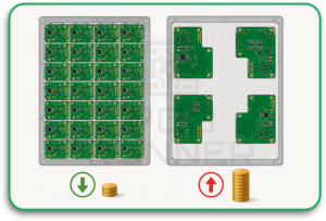
Improve Panelization for Better Cost Efficiency
What Is PCB Panelization
Panelization is the process of arranging multiple copies of your board on a single manufacturing panel. Fabricators charge per panel, not per board. Fitting more boards per panel directly reduces cost per unit.
Maximising Board Usage on Panels
Work with your manufacturer on panel utilisation before finalising board dimensions. Sometimes adjusting your board outline by 2–3 mm changes how many copies fit on a standard panel, and that difference compounds significantly at production volumes.
Reducing Material Waste
Irregular board shapes, L-shapes, cutouts, non-rectangular outlines, waste panel area and create routing debris that slows production. Rectangular or square boards with clean outlines maximise panel utilisation and minimise material waste. If your mechanical requirements require an irregular shape, design in a V-score or tab-rout break-off to minimise wasted area.
PCB Runner Guide To PCB Panelization For Cost Reduction
Panelization is one of the simplest ways to reduce PCB cost, but it is often reviewed too late. A board may be electrically correct and still waste space on the production panel. That wasted area becomes wasted material, machine time, and money.
PCB Runner helps teams review panel fit before the board outline is fully locked. Even a small change in board length, width, corner shape, or break-off tab placement can improve how many boards fit on a standard panel.
Good panelization should consider:
- Board shape
- Edge clearance
- V-score or tab-routing method
- Component placement near edges
- Handling space for assembly
- Fabricator panel size
- Expected production volume
The goal is not to shrink the board blindly. The goal is to use the panel better without hurting assembly, testing, or reliability.
Optimise Component Selection and Placement
Using Standard and Readily Available Components
Standard components, 0402 and 0603 passives, common SOT and SOP packages, widely sourced ICs, are cheaper to buy, faster to source, and easier for automated assembly equipment to handle. Non-standard components add BOM cost, extend lead times, and slow down pick-and-place programming.
Reducing Unique Component Count
Each unique component requires its own feeder, tape reel, and placement program entry. If two different resistor values in your design can both be replaced by a single intermediate value without affecting performance, eliminating one of them reduces assembly setup cost and simplifies your BOM.
Placement Strategies That Simplify Assembly
- Place all SMT components on one side of the board where possible, double-sided SMT requires two reflow passes
- Orient all polarised components consistently, it speeds up AOI programming and reduces placement errors
- Keep components away from board edges, minimum 3 mm clearance prevents damage during depaneling
- Group components by function, it simplifies inspection and makes rework easier when needed
Design for Manufacturability (DFM) to Reduce Costs
Following Manufacturer Design Guidelines
Every fabricator publishes design rules, minimum trace widths, minimum via sizes, copper-to-edge clearance requirements. These rules represent their actual process capability. Designing within them produces boards that build cleanly. Designing outside them produces engineering queries, yield loss, and schedule delays.
Avoiding Design Errors That Cause Rework
Solder bridges from inadequate pad spacing, tombstoning from asymmetric pad design, and cold solder joints from missing thermal reliefs are all design errors that cause assembly rework. Rework is expensive, far more expensive than the design review that would have prevented it.
Improving First-Pass Yield in PCB Manufacturing
First-pass yield is the percentage of boards that pass inspection without rework. Every percentage point of yield improvement reduces cost. A DFM-optimised PCB design consistently achieves higher first-pass yield than one that was never reviewed for manufacturability. At production volumes, the cumulative cost difference is substantial.
Minimise Drilling and Via Costs
Reducing the Number of Vias
Every via requires a drilled hole, copper plating, and potentially solder mask coverage. Vias add cost per unit. Reducing via count through better routing, using longer traces to avoid vias where possible, reduces cost without affecting function.
Avoiding Blind and Buried Vias When Not Needed
Blind vias (connecting an outer layer to an inner layer without going through the full board) and buried vias (connecting inner layers only) require sequential lamination, a separate lamination and drilling cycle before the full board stack-up is completed. This significantly increases fabrication costs and time. Use through-hole vias wherever the design allows.
Standardising Drill Sizes
Using a wide variety of hole sizes forces multiple drill tool changes during production. Standardising on the minimum number of hole sizes needed, typically two to three for vias and component holes, reduces drill setup time and speeds production.
Optimise Solder Mask and Finishing Options
Choosing Cost-Effective Surface Finishes
ENIG (Electroless Nickel Immersion Gold) is the most commonly over-specified finish. It is excellent for fine-pitch SMT and for applications that require long-term flat, solderable surfaces. For boards using standard through-hole components or larger SMT packages, lead-free HASL provides adequate solderability at significantly lower cost.
Avoiding Complex Mask Requirements
Solder-mask-defined (SMD) pads, where the mask opening is smaller than the copper pad, require more precise mask registration and incur additional cost. Non-solder-mask-defined (NSMD) pads are easier to produce and are preferred for most SMT applications. Use SMD pads only where the design genuinely requires it.
Reduce Assembly Costs Through Smart PCB Design
Designing for Automated Assembly
Automated pick-and-place assembly is dramatically cheaper per component than manual placement. Design your board so that all SMT components are accessible to standard assembly equipment, adequate spacing, consistent orientation, no components hidden under other components or in recessed areas.
Avoiding Manual Soldering Where Possible
Manual soldering costs roughly ten to twenty times more per joint than automated reflow. Every through-hole component that an SMT equivalent could replace reduces manual assembly time. When through-hole components are required, group them to minimise hand-soldering passes.
Consistent Component Orientation
When all polarised components share a consistent orientation, all capacitors with positive terminals in the same direction, all ICs with pin 1 in the same corner, automated inspection runs faster, programming is simpler, and human verification is easier. This costs nothing to implement in layout and saves real time in production.
Prototype and Test Before Mass Production
Testing your design with a small prototype run before committing to production quantities is always the right decision economically. A design issue found on ten prototype boards costs the price of ten boards to fix. The same issue found after a 5,000-unit production run costs the price of 5,000 boards, rework, and a schedule delay.
Prototype builds also validate your DFM assumptions, confirming that the manufacturer can actually achieve the tolerances you specified and that the assembly process works as intended.
Work Closely With Your PCB Manufacturer
Getting Early Feedback on PCB Design
Share your design intent, target specifications, and production volume with your manufacturer before layout is complete. A manufacturer who understands your requirements can flag cost issues while they are still easy to fix, not after the design is frozen.
Understanding Manufacturing Capabilities
Different manufacturers have different process capabilities and different cost structures. A manufacturer optimised for high-complexity low-volume work will price a simple two-layer board differently from one optimised for high-volume standard production. Match your manufacturer to your design type, not just to the lowest quote.
Adjusting Design Based on Real Constraints
PCB Runner consistently sees the value of this early engagement. Designers who understand their manufacturer’s actual stack-up options, material stocks, and drill capabilities make better layout decisions, and their boards cost less and build faster as a result.
Common PCB Design Mistakes That Increase Costs
Overcomplicating the Design
Adding layers, vias, or component variety beyond what the design actually requires is the most common cost mistake. Complexity for its own sake never helps.
Ignoring Manufacturing Constraints
Designing traces thinner than the manufacturer can reliably etch, or specifying tolerances tighter than their process can hold, results in yield loss and rework that cost far more than a slightly more conservative design would.
Last-Minute Design Changes
Changes made after fabrication files have been released, or worse, after panels have been ordered, are extremely expensive. An engineering change at the layout stage costs an hour. The same change after production has started can cost weeks and thousands of dollars in scrap and retooling.
PCB Design Decisions That Cause Expensive Prototype Respins
A prototype respin is one of the most frustrating costs in PCB development. It delays testing, slows product launch, and often forces engineers to repeat work that could have been avoided.
Many respins are caused by design choices that look minor during layout. Poor thermal reliefs, tight spacing, wrong footprint selection, weak grounding, and unclear manufacturing notes can all lead to board problems.
Common causes of prototype respins include:
- Incorrect component footprints
- Poor connector placement
- Insufficient clearance around high-voltage areas
- Weak ground return paths
- Missing test points
- Overly tight routing near critical signals
- Incorrect drill sizes
- Poor thermal planning
- Ignoring manufacturer design rules
A design review before file release is far cheaper than discovering these issues after the boards arrive.
Best Practices for Cost-Optimised PCB Design
Plan for Cost From the Start
Include cost as a design constraint from day one, alongside electrical performance, mechanical requirements, and thermal management. Cost is not something you optimise at the end. It is something you design from the beginning.
Keep Design Simple and Standardised
Use the minimum layer count that meets your requirements. Use standard materials, components, via types, and tolerances wherever possible. Simplicity is not a compromise, it is an engineering discipline applied to cost.
Balance Performance, Cost, and Manufacturability
Optimising PCB designs means finding the point at which performance requirements are fully met, manufacturing risk is minimised, and unit cost is as low as the design allows. That balance point exists for every design. Finding it requires deliberate analysis, not defaulting to whatever seems safest or most familiar.
Cost Optimisation Checklist Before Sending PCB Files To Manufacturing
Before sending PCB files to manufacturing, review the design for cost, reliability, and build readiness. This final check can prevent avoidable questions, delays, and rework.
Use this checklist before releasing Gerber, drill, BOM, and assembly files:
- Confirm the layer count is necessary
- Check whether standard FR-4 is suitable
- Review board size for panel utilisation
- Reduce unnecessary vias where possible
- Avoid blind and buried vias unless required
- Standardise drill sizes
- Check trace width and spacing against fabricator rules
- Confirm surface finish matches the real need
- Review component availability
- Reduce unique component count where possible
- Add enough test points
- Keep components clear of board edges
- Confirm polarity marks and silkscreen labels
- Run DRC and DFM checks
- Share files with the manufacturer for early review
This checklist helps catch cost problems before they enter production. It also gives the manufacturer cleaner files to work with.
Conclusion
PCB cost is not something that happens to you in manufacturing, it is something you design in, or design out, long before the board reaches the factory.
Every layer count decision, every material choice, every via type, every component selection, and every tolerance specification either adds cost or controls it. The engineers who understand this consistently produce boards that perform well and cost less to build, not by compromising, but by designing deliberately.
PCB Runner supports design teams through exactly this process, from early design review through prototype validation and into cost-efficient production.
“The most expensive PCB is the one that has to be redesigned. Get the design right the first time, and build cost-efficiency in from the start.”
FAQs
What Is the Biggest Cost Factor in PCB Manufacturing?
Layer count is typically the single biggest cost driver. Every additional layer adds lamination, drilling, and processing costs that compound quickly. After layer count, board size and via types, surface finishes, critical trace line & spacing are the next most significant factors.
How Can I Reduce PCB Cost Without Affecting Quality?
Focus on eliminating complexity that does not serve a functional purpose, unnecessary layers, over-specified materials, blind vias where through-hole routing would work, and exotic surface finishes when standard finishes are adequate. Quality comes from appropriate design choices, not expensive ones.
Does Reducing Layers Always Lower Cost?
Generally, yes, but not always. If reducing layers forces trace routing that compromises signal integrity and causes a respin, the cost of the respin exceeds the savings from fewer layers. Reduce layers only when performance requirements can genuinely be met with fewer.
How Important Is DFM for Cost Optimisation?
DFM is central to cost optimisation. A DFM-compliant design yields higher yields, requires less rework, and moves through production faster than one that was never reviewed for manufacturability, the cost difference between a DFM-reviewed and non-reviewed design compounds significantly at higher production volumes.

