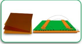
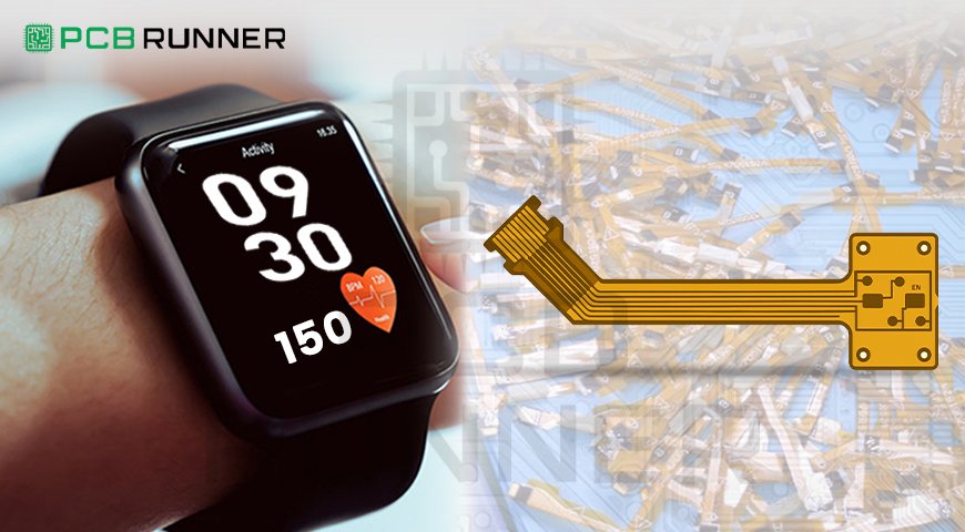
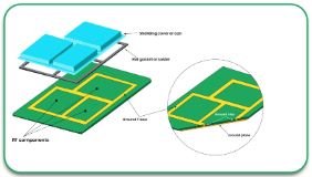
Effective and efficient planning of PCB routing directly influences the PCB board assembly work. Effective routing ensures optimal signal flow, reduces interference, and improves thermal and overall circuit performance. In all types and levels of PCBs, from single boards and multilayer systems, manufacturers adhere to strict PCB routing policies.
Routing involves planning trace paths, spacing between conductors, and stacking layers in a manner that facilitates the easiest path for signal flow and cooling. Routing issues can deteriorate signal strength, increase EMIs, and reduce overall dependability.
In this article, we will discuss essential PCB routing best practices and rules, sophisticated techniques in PCB fabrication to enhance circuits within designed bounds, and other cutting-edge techniques and technologies.
If you need precise route crafting for your CAD designs, contact PCB Runners and let professionals handle the work.
What is PCB Routing?
Connecting the different components of a circuit entails routing, which involves placing traces for the electrical pathways that convey the signal and power. These pathways are referred to as traces, and routing techniques can make use of multiple boards, and via placement out of alignment for prevention of crosstalk, noise, and interference that form wires in close proximity to one another.
Cutting-edge PCB design software and automation systems allow modern manufacturers to efficiently optimize complex circuit routing based on performance metrics and ease of manufacture.
PCB Design Guidelines
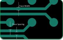
Trace Width and Spacing
- Proportions of Trace width for current capacity must be balanced.
- Reduction of resistive heat and increased thermal output is seen with broader electrical pathways.
- Standard spacing avoids signal overlapping and cross-wiring.
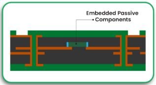
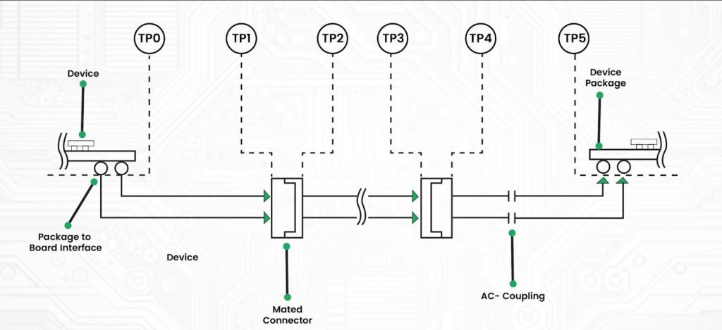
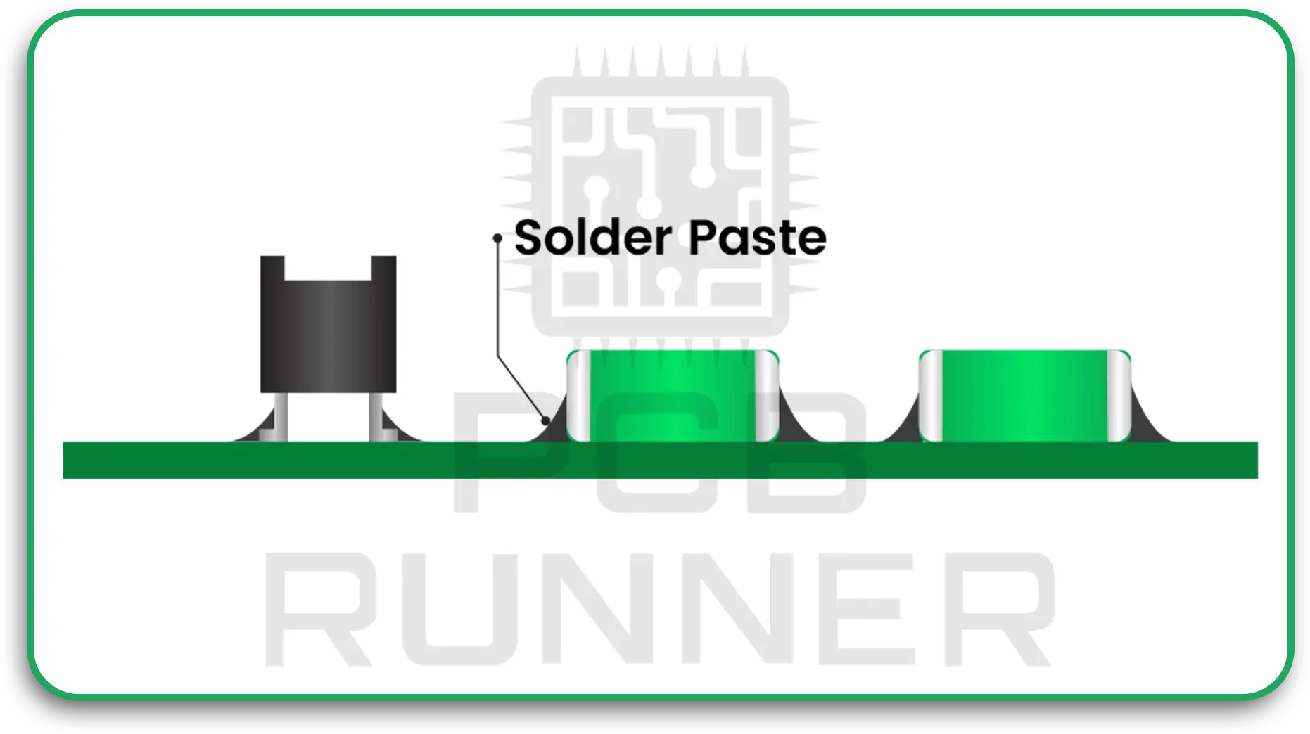
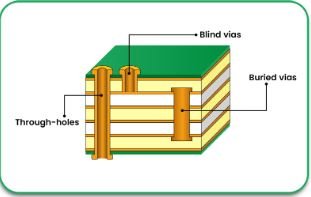
Vias Types and Placement
Different levels of a PCB board can be interconnected with Vias. The common types of Vias are:
- Through-Hole Vias – These pass through the entire board.
- Blind Vias – These connect inner layers with outer layers.
- Buried Vias – These only connect internal layers.
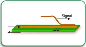
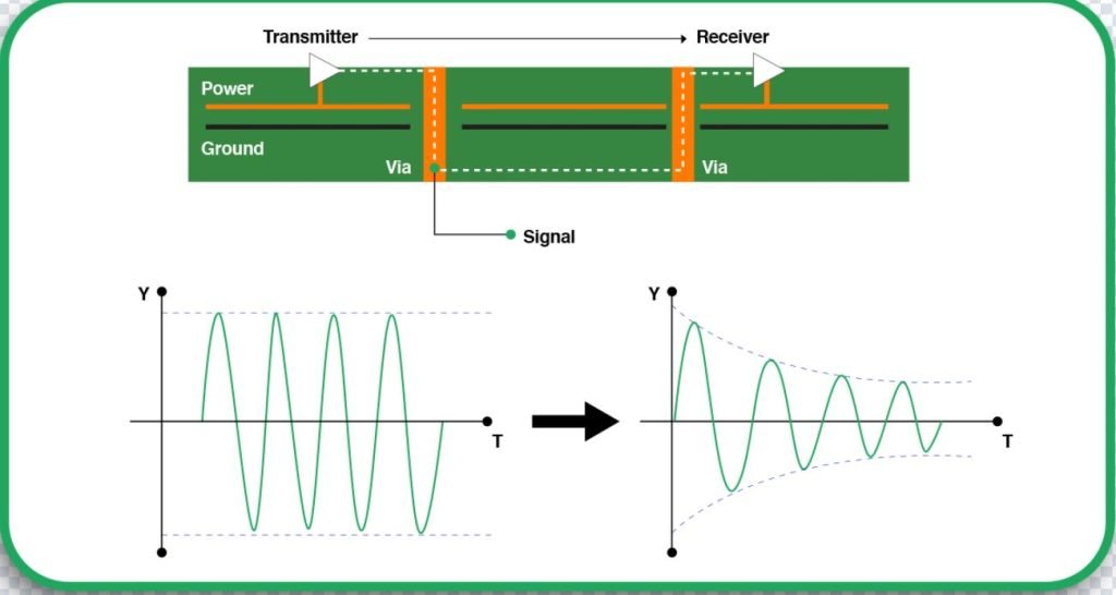
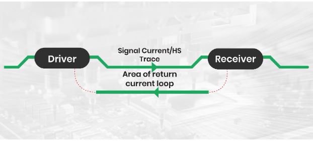
High-Speed Routing and Signal Integrity
- To lower signal bounce, sharp angles greater than 45° should be avoided.
- For the transmission of high-speed data, the routing of differential pairs should be employed.
- Traces pertaining to the clock and other high-speed signals should be short and direct.
Ground and Power Planes
- The placement of defined ground and power planes minimizes noise and maximizes efficiency.
- Elimination of interference is encouraged while keeping the planes as continuous as possible.
- Altering the portion of the ground plane could lead to EMI difficulties.
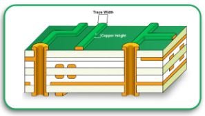
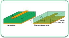
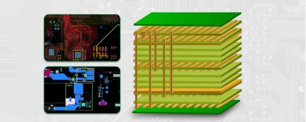
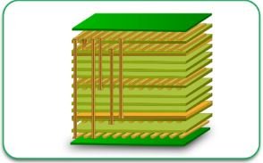
Multilayer PCB Stack-up Layers
- An immediate advantage of using multilayer PCBs is improved routing versatility for densely packed components.
- Interchange the Power/ground layer with signal layers and vice versa for reduced interference.
- For mechanical strength, ensure the stack-up layers have symmetry.
Best Practices for PCB Routing
Focus on Component Placement
Before beginning to PCB route, make sure to place components appropriately. Try to:
- Integrate associated components (for example, power circuits and signal paths).
- Minimize interference by bringing high-frequency components closer together.
- Provide adequate space for connectors and mounting holes.
Refine Trace Routing
Maintain ease of manufacture and orderliness with your PCB trace routing:
- Direct routing should be to the point and as short as possible.
- Glance at the 45° rule. 90° bends are too sharp.
- Balance spacing between traces that are close to each other to avoid crosstalk.
Don’t Route Over Split Planes
- Sustain return paths by preventing signals from running over split power or ground planes.
- Enhance EMI shielding through the use of ground fills and stitching vias.
Thermal Management Issues
- Use thermal relief pads to disperse heat in high-power designs.
- Ensure power traces are dispersed evenly to prevent overheating.
- The use of thermal vias may be considered in order to enhance heat dissipation.
Observe DFM Policies
- Make sure that traces, vias and pads are within the PCB routing guidelines for manufacturing.
- Clearances suitable for soldering and assembling must be provided.
- Prevent routing vias in close proximity to component pads, as this will cause solder wicking.
Advanced Techniques in PCB Routing
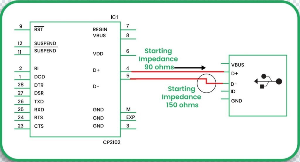
Differential Pair Routing
For USB, HDMI, and Ethernet signal routing, the following apply:
- Use the same trace width and spacing throughout.
- Pair routes with the same length to maintain signal integrity.
Controlled Impedance Routing
- Minimizes signal reflections in RF and high-speed digital circuits.
- Calculation of trace width and spacing needs precision based on board material properties.
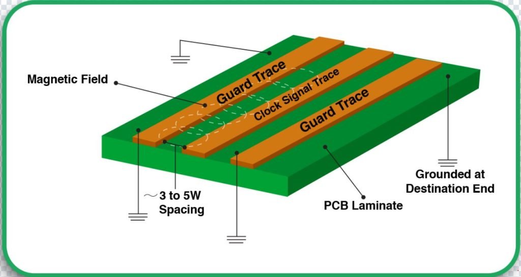
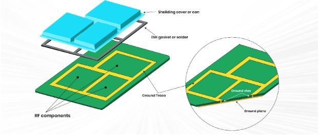
Via Stitching for EMI Shielding
- Placing vias along the signal trace helps reduce EMI.
- Common in RF and sensitive analog circuit designs.
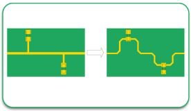
Length Matching for Synchronized Signals
- Ensure equal trace lengths for clock signals and data signals so they arrive at the destination at the same time.
- Use serpentine routing to equalize lengths if needed.
The Role of PCB Manufacturers in Routing Optimization
Manufacturers of PCBs have significant experience, which helps in optimizing routing for PCB board assembly and performance. With the use of sophisticated techniques in the fabrication of PCBs, these manufacturers are able to:
- Give suggestions about the design with the aim of enhancing the routing.
- Comply with the rules of PCB routing set for manufacturing.
- Modify trace layouts designed for speed and power consumption.
- Fix errors using design rule check (DRC).
Conclusion
Following best practices in PCB routing is essential in achieving optimal performance, reliability, and manufacturability in circuit board design. Engineers can successfully improve trace layouts, reduce crosstalk, and the overall signal integrity through proper trace routing techniques.
Working with a proven and established PCB manufacturer helps maintain compliance with the design rules of the PCB routing which enhances the efficiency of upwards of PCB board assembly and the quality of the end products.
Are you looking for assistance in routing and fabricating advanced PCBs?
For tailored professional solutions in PCB fabrication, routing, and multilayered PCBs, Trust PCB Runners.
FAQs
What does routing on a PCB mean?
Routing consists of the placement and layout of the electrical traces that connect various components on the PCB.
What makes important computer-aided manufacturing routing guidelines?
Routing guidelines assist in maintaining proper signal conveyance, limiting outside signals, and manufacturability.
What are the common PCB routing rules for manufacturing?
Common routing rules include appropriate solder mask openings, transverse trace clearance, and spacing on traces.
What benefits do multilayer PCBs offer for routing?
Multilayer PCBs provide better separation between the signal, power, and ground layers, thereby decreasing interference and boosting performance.
What are the best PCB routing techniques for high-speed signals?
For high-speed designs, use differential pair routing, controlled impedance, length matching, and via stitching to maintain signal integrity.