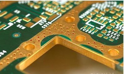
The metallization of a circuit board’s edges is known as side plating, sometimes known as edge plating or Castellation, in the PCB industry. Stated differently, side plating is the copper plating that extends along one or more of the board’s peripheral edges and from the top to the bottom surface. Any surface treatment that offers electrical connectivity can be used for side plating, including HASL, ENEPIG, and ENIG. The printed circuit board’s edge is utilized for the technical aspects of the subsequent assembly when side plating is applied. The PCB’s interior spaces and some of its exterior can be metalized.
In order to ease electrical connections, exposed copper connections around the borders of a printed circuit board (PCB) are plated with a metallic coating, such as tin or gold. A thorough explanation of PCB edge plating is given in this article, along with information on edge connector types, plating procedures, inspection, reliability considerations, and upcoming trends.
PCB Edge Plating Advantages:
1. Improved Current Conduction:
A higher current carrying capacity enhances the quality and dependability of the board. In addition, the right amount of conduction safeguards delicate edge connections while enabling components to function as needed.
2. Integrity of Signal:
By reducing interference from entering the internal electrical pulse transmission, edge plating improves signal integrity.
3. Dispersion of Heat:
The metallic nature of the plated edges provides an extra cooling surface area that is utilized to release heat into the surrounding air. The metallic surface increases the board’s dependability, particularly when parts are heat-sensitive.
4. Improved Performance of EMC/EMI:
Sterilized edges stop random electric and magnetic fields by letting stray currents pass through.
5. Enhance Compatibility with Electromagnetic Fields:
Enhancement of electromagnetic compatibility through edge plating
6. Avoid Injury from Electrostatic Fields:
Static electricity can damage delicate components while handling circuit boards, however, metal surfaces can help absorb static electricity.
Challenges in Edge Plating PCBs
As previously discussed, accurate handling of the PCB circuit boards is crucial for PCB edge plating. A small error can lead to a number of issues, including burr formation and the copper peeling phenomenon. And then there is a significant risk from the two circumstances. Let’s now examine various PCB edge plating constraints, which are signed prior to the fabrication process, in addition to the specific understanding of the application range of PCBs.
Copper Peeling:
Insufficient adhesive strength of the plating on the large substrate surface is the cause of the copper peeling. The difficult challenge can be overcome by employing chemical and proprietary methods to roughen the surface.
Burrs:
During the final machining step of PCB edge plating, specifically the milling process, burrs are frequently generated, especially on castellation holes. To smooth out the edges of the feature, we use the particular and adapted process flow for this task.
There must be some spaces where route tabs are placed. The manufacturer is unable to plate the entire edge because the circuit boards inside the production panel of the PCB prototype must be fixed. Before beginning the through-hole plating process, the outlines that need edge plating must be routed in order to fabricate boards with edge plating. V-cut notches on circuit boards that need edge plating are thus ruled out.
The edge plating technique necessitates meticulousness in order to overcome plating laying problems. To perform an edge plating procedure correctly, you need specific tools and a reasonable level of experience. A PCB edge needs to be handled carefully and prepared before plating in order for the plating to adhere to it. For the duration that the board is in use, the plating must stay fixed to the edge. In addition, care must be taken during the edge plating soldering process to prevent harm to the interlayer through-hole connections. The procedure to stop burrs from forming is given the highest priority. A board can fail catastrophically due to burrs.
PCB Runner’s PCB Manufacturing and Prototype Services
The most reputable and trustworthy option for full-feature printed circuit board creation is Pcb Runner at PCB Manufacturer in the UK since we provide a range of board sorts and have an incredibly flexible approach to problem-solving.
|
Parameters |
Specifications For Rigid |
Specifications For Flex |
|
Edge plating with thickness |
20 um copper on edge plating |
15um |
UK and Europe’s (Luxembourg’s) Complete Feature Circuit Board Manufacturing Capabilities
- Fast Turnaround
- Prototype
- Widespread Manufacturing
- Special Services at No Cost
- Audits for DFM and DFA
- Penalization
- Electrical Examination
- Creating Stencils
- Personalized Layer Stack-up
- Consultation to lower the cost of board production.
- Streamlined Circuit Assembly

Typically, the edge plating of PCBs entails:
- Making holes to receive edge contacts
- Electroless and then electrolytic plating of copper
- Etching to create distinct traces
- Surface preparation techniques such as micro etching
- Immersion plating of metal, such as gold
- Sanitizing and then drying the boards
- Examining the quality: thickness, continuity, and flaws
- If necessary, electrical testing
Standard PCB techniques plus final plating are typically used during fabrication.

Ref: Altium edge plating
Quality Control for Edge Plating
Essential process controls required:
Plating Thickness:
Use X-ray fluorescence or microscopy to verify that the minimum thickness is met. Poor plating raises the possibility of corrosion or wear.
Continuity:
Use plated edge contacts to confirm electrical connectivity from the inner layers.
Plating Coverage:
Look for spaces or thin spots near traces.
Over Plating:
Take care that the glass weaving does not receive an excessive amount of plating can prevent reproduction.
Trace Geometry:
Verify that dimensions match specifications by using trace geometry.
Applications of Edge Plating PCBs
PCB Edge-Plating in the Communications Industry
With satellite communication, internet access, and mobile communication all included, the communication industry is one of the fastest growing in the world. The transmission of signals must be stable and fast in these domains. By encasing signal layers in gold plating, Edge Plating PCB reduces the possibility of signal loss and interference and provides exceptional signal transmission performance. This feature makes sure that communication devices continue to function exceptionally well in a variety of environmental settings, ensuring consistent connectivity and high-quality conversation.
Medical Device Applications
Precision and dependability are critical in the medical industry. Medical gadgets, such as monitoring devices, implantable medical devices, and medical imaging equipment, frequently use edge plating printed circuit boards. The necessity for these devices to function in damp, hot, or humid conditions highlights the importance of PCB durability. In addition to offering exceptional connectivity, Edge Plating PCB can survive severe environmental conditions, guaranteeing the precision and long-term dependability of medical equipment.
Automation and Control in Industry
Devices used in industrial control and automation must be able to function reliably in situations with high temperatures, high voltages, and significant electromagnetic interference. The Edge Plating PCB’s design makes it resistant to damage and corrosion in these harsh environments. It also offers greater current capacities, which makes it extremely beneficial for industrial power transmission. With less maintenance and downtime, this PCB technology helps to increase the efficiency and dependability of industrial automation systems.
Quality and Compliance
With certifications in both ISO 9001:2015 and ISO/TS 16949:2009, PCB Runner, a PCB manufacturer located in the Netherlands, provides fabrication and assembly services. Regardless of whether the circuit board is a prototype or is being produced in large quantities, our straightforward objective is to provide our clients with guidance and support about their board needs and to manufacture them promptly, with superior quality, and with first-rate customer care.
We supply boards all around Europe, the UK, and the rest of the world from our base in the Netherlands. In addition to providing complete PCB design and manufacturing services, we also offer product construction, test, SMT and PTH assembly, and cable assemblies.
A one-stop shop for circuit board
With a focus on client satisfaction, PCB Runner, PCB assembly Netherlands, provides contract manufacturing for electronic assemblies. Our main offering to clients is a one-stop shop for circuit board, circuit assembly, box and system builds, and all associated engineering services, from concept to production.
Electronic contract manufacturing
From design through mass production, PCB Runner offers our clients full electronic contract manufacturing services. Our goal is to be the most productive and successful supplier of all services related to electronic manufacturing. Customers are pleased that a single provider, totally dedicated to quality and customer satisfaction, can manage all of their assembly-related demands.
Why Choose PCB Runner for Edge Plating PCBs
The Netherlands-based PCB maker is aware that every client and their needs are unique and distinct. Customers need to be able to trust their source to fulfil their needs, in our opinion. Our speciality is assisting clients in launching their goods into the market as quickly as feasible.
One of the rare businesses that actually manufactures boards in-house is PCB Runner. We manufacture every kind of board, including:
- Aluminum-based metal PCBs
- PCBs using Rigid-Flex (FR-4 and Polyimide)
- Board flex (polyimide)
- Through-holes, SMT, BGA, and other HDI boards
- Lead-Free Boards that Comply with WEEE and RoHS
- Intel PCB Mil spec (IPC Class 1, 2, 3).
- 40+ layer multi-layered circuit boards
- Materials for Boards: FR-4, Polyimide, Rogers, and Others
- Spacing and Trace to 3 mils
- Blind and Buried vias
- Filled vias Boards with Heavy Copper Via-in-Pad
- Skilled Assembly and Fabrication Services
In addition to the aforementioned, we provide professional manufacturing and assembly services for:
- Prototype circuits
- Board Runs
- Small and Medium
- Quick Turn PCBs
- Burn-In for Boards
Read More: Solving Common Issues in Edge Plating PCBs Tips and Tricks
Conclusion
In conclusion, a variety of industries use PCB edge plating and connections as a flexible and affordable interconnection solution for interchangeable subsystems, cards, and modules. Edge connectors will continue to be able to fulfil the demands of thinner boards, faster signalling, denser contacts, and enhanced reliability because of continuous improvements in board materials, plating technology, and precision production processes. Although there are other options, such as board-to-board connectors, edge connectors’ ease of use and simplicity guarantee their continued use whenever field replaceability of circuits is needed long into the future.
PCB Runner offers custom design edge plated technology manufacturing layout services for all industries and critical design requirements. Please submit your schematics & BOM files to our email at sales@pcbrunner.com or engineering@pcbrunner.com

