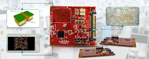
Even your smartphone and laptop make use of a PCB (Printed Circuit Board). Circuit boards are essential in electronics, providing a platform for all components as well as ensuring the devices operate effectively. But have you ever asked yourself the question: how were those boards manufactured?
The PCB manufacturing process is complicated and consists of several phases, from conceptual design to final evaluation. Knowing these processes can help professionals make better choices, be it an engineer, hobbyist, or even an establishment seeking a trustworthy PCB board manufacturer.
This blog will provide everything from seeking information on the newest industry advancements and innovations to what PCB fabrication is. We will also disentangle the steps that explain how to fabricate PCB, as well as cover the sophisticated technologies high-density interconnect PCB manufacturers employ to produce next-gen circuit boards.
What is PCB Fabrication?
Through fab processes, designers can break down their schematic into portions; fabrication can be defined as the step of transforming a design into an actual physical circuit board. It includes the laying out of the copper traces, drilling the relevant holes, and putting protective layers before the components are put together.
The PCB Manufacturing Process
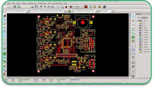
1. PCB Design and Layout
Before any construction can start, soldering components to a PCB requires a basic layout to have been previously done in CAD or CAM PCB design software. This defines the location of electrical elements and connecting wires.
2. Material Selection
The following step is a selection of appropriate PCB board material. Some of the more important options are:
Fibreglass Reinforced Epoxy FR-4: Used as the base standard for most boards.
Metal Core: Used for LED lighting as well as power electronics because they dissipate heat.
Polyimide: Used for flexible PCBs due to its flexibility and capability to withstand high temperatures.
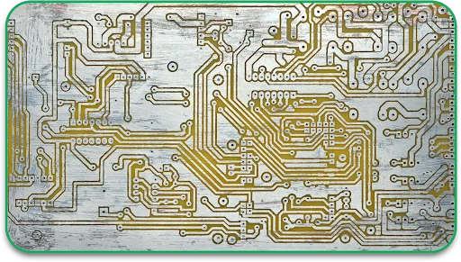
3. Printing the Circuit Design
The design is printed on the board with a photoresist technique that engraves the design into the copper covering the board.
4. Etching Process
Etching is the process used to remove the extra copper while retaining the etched paths. This can be done in two primary manners:
Wet Chemical Etching: Uses acid solutions to get rid of any unwanted copper.
Dry Etching: More accurate material removal is done by the use of lasers or plasma.
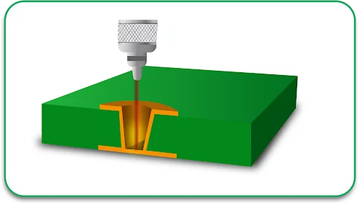
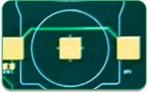
5. Drilling Holes
Holes are drilled on the multilayer boards to facilitate interlayer connections and to mount surface-mounted components. To make microvias in high-density interconnect PCBs laser drilling is used which significantly improves signal performance.
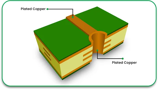
6. Plating and Copper Deposition
To create electrical connections between the layers, copper is plated onto the holes. This step is done after drilling.
7. Solder Mask and Silkscreen Application
A silkscreen layer provides a way to label components, while a solder mask layer is meant to protect copper traces from oxidation and short circuits.
8. Surface Finishing
There are various surface finishes added on a PCB to improve the durability and solderability of the PCB, such as:
HASL (Hot Air Solder Leveling) – very cheap but not very durable, so its lifespan is short.
ENIG (Electroless Nickel Immersion Gold) – is used for high-reliability applications, which is very common.
Immersion Silver/Tin – available for other specialized needs.
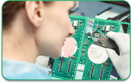
9. Quality Control and Testing
These boards go through numerous testing procedures to guarantee quality before shipping, for example:
Automated Optical Inspection (AOI): checks the board for defects visually.
X-ray Inspection: determines whether or not there are any issues with the hidden layers of the board.
Electrical Testing: checks to see if the circuitry within the board works.
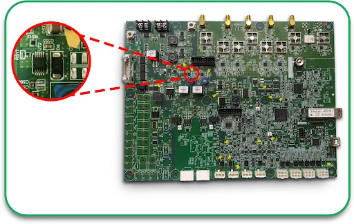
10. Final PCB Assembly
When the board passes the testing phase, the components are then soldered onto the board utilizing:
Surface Mount Technology (SMT) – common with modern electronics devices.
Through-hole technology (THT) – is used in industrial electronics because it’s more durable.
Key PCB Manufacturing Methods
1. Traditional Etching (Subtractive Process)
Best For:PCBs that are either single-layer or double-layer of standard forms.
Pros: Cheap and reliable, so a lot of people make use of it.
Cons: Not highly precise hence difficult for high-concentration designs.
2. Additive Manufacturing (3D-Printed PCBs)
Best for: Custom designs and prototypes
Pros: Short lead times and Produce little scrap material.
Cons: Not well suited for large quantity production.
3. HDI PCBs – High-Density Interconnect PCBs
Best for: Electronics requiring high performance in small devices.
Pros: Smaller devices can be made while increasing signal quality.
Cons: Increased unit manufacturing cost.
4. Rigid-Flex and Flexible PCBs
Best for: Wearable devices, Automotive, Aerospace.
Pros: Durable and lightweight.
Cons: Special handling and materials needed.
5. MCPCB – Metal Core PCBs
Best for: Devices that require a lot of power, such as LEDs and power supplies.
Pros: Outstanding heat dissipation.
Cons: More weight than other PCBs.
Innovations in PCB Manufacturing
1. AI-enhanced PCB Design:
The use of machine learning assists in optimizing circuit layouts by reducing defects while increasing efficiency.
2. Laser Drilling for HDI PCBs:
A laser’s use of ultra-small vias allows for high-speed and compact PCBs.
3. Eco-Friendly PCB Manufacturing:
New techniques use water-based etching combined with lead-free soldering, reducing pollution.
4. Hybrid PCBs:
Combining rigid and flexible layers results in more durable and better-performing advanced electronics.
Choosing the Right PCB Manufacturer
1. Years of Operation and Industry Experience
Seek a PCB board manufacturer that has worked with your industry, whether it be consumer electronics, medical technology or aerospace.
2. Manufacturing Capabilities
Choose from PC board manufacturers that are able to do HDI, multilayer, and flex PCB fabrication.
3. Certifications and Quality Standards
A good PCB manufacturer must obtain the following:
- ISO 9001 certification for Quality Management.
- Compliance with IPC Standards for reliability of boards.
- Compliance with RoHS standards for environmentally friendly manufacturing.
4. Costs and Speed of Production
Analyze costs and lead times to determine the best value for your work.
5. Customer Support
A competent PCB manufacturer should offer responsive technical and design support.
Future Trends in PCB Manufacturing
PCBs design and manufacturing is expected to change with the onset of new technologies. Some of the changes you may want to monitor include:
- PCBs are designed for 5G and IoT connectivity.
- PCBs are made with nanotechnology for super slim, lightweight, and high-performing boards.
- Smart factories with automated systems will improve the speed and accuracy of production.
Conclusion
The variety of methods and technologies available for PCB manufacturing has increased tremendously. No matter if you need high-density interconnect PCBs, flexible circuits or custom multilayer boards, a good pcb board manufacturer is always the answer for quality and performance.
Take the first step toward your next project and reach out to PCB Runners for top-tier fabrication of PCBs using modern technology and quick service times.
Frequently Asked Questions (FAQs)
1. What is PCB fabrication?
PCB fabrication is a process of making circuit boards, which is composed of the decision-making processes on materials, etching, drilling and plating.
2. What is the primary difference between HDI PCBs and standard PCBs?
The main difference is that the HDI PCBs have smaller component yields and microvias, which grant them better signal performance and component density.
3. What materials are used for manufacturing of PCBs?
Such materials as FR-4, aluminium, ceramic, and polyimide are the most common, but the selection depends on the application.
4. What is the best PCB manufacturing method?
That depends on your needs. Etching for standard boards, HDI for compact designs, and flex for wearable devices.
5. How do I choose the right PCB manufacturer?
You look for experience, certifications, advanced capabilities, and strong customer support.

