The development of devices that are deeply integrated with modern technology begins with PCBs. Hence, Printed Circuit Boards and their designs are necessary to create a low-cost, high-performance product that is reliable in the long term. Custom PCBs are made to cater to varying industry needs, from consumer-based electronics to industrial-grade machinery.
The emergence of PCBs with software-based electronic circuits has made it possible for designers to design more efficient, compact, and powerful PCBs. This article examines the critical issues with regard to the optimization of electronic PCBs from layout design, material choice, signal integrity, and even thermal management.
Important Aspects in PCB Optimization
1. Trace Length and Positioning Design
The layout is key to reducing trace length and increasing overall performance. The right placement of components improves signal delay and minimizes interference and overall performance. This includes:
- Trace Grouping: If the components are grouped, the trace length will be reduced significantly.
- Trace Composition: Grouping signals can be improved by applying differential pair and shortest distance routing.
- Power and Ground Planes: When power and ground layers are allocated, currents are more effectively distributed, and electromagnetic emissions are also minimized.
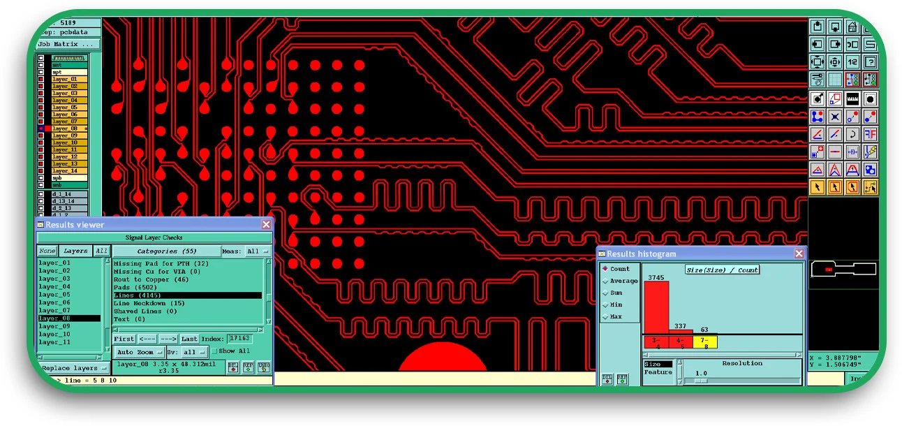
2. Choosing the Best Material
The mechanical aspects of the PCB, such as thermal conductivity, signal durability and strength, and transmission, are very reversible. Here are some common materials used:
- FR-4: The industry standard for PCBs. Socioeconomically beneficial. Good electrical performance.
- Polyimide: Ideal material for flex PCBs because of its flexibility and heat resistance.
- Rogers Laminates: Employed in non-microwave frequencies because of its low signal attenuation.
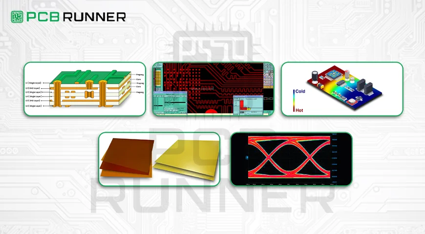
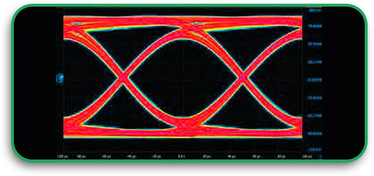
3. Signal Integrity Issues and High-Speed Design
Signal integrity needs to be maintained in high-speed PCBs to avoid blurring and information loss.
- Impedance Matching: Guarantees no reflection or loss of signals.
- Crosstalk Reduction: Adequate space between traces reduces unwanted signal interference.
- Shield and Ground: Proper grounding of devices reduces EMI problems.
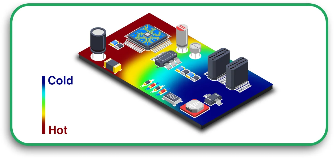
4. Thermal Management
Great care must be taken to control heat, as uncontrolled heat buildup can cause severe component damage.
- Heat Sinks and Vias: Aid in drawing away heat from critical components.
- Thermal Pads and Conductive Adhesives: Improve the transfer of heat to the cooler parts.
- Component Positioning: Positioning of heat-producing components helps to reduce excessive localized heating.
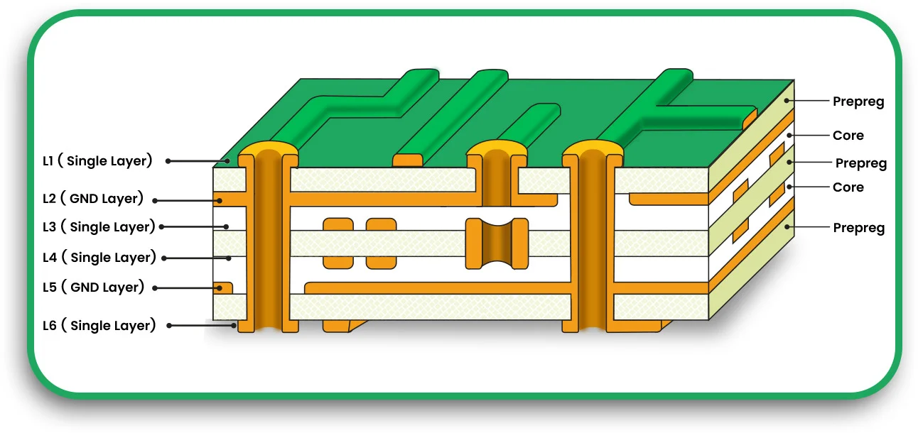
5. Multi-Layer PCB Design
In complex designs, the use of multi-layer PCBs has the following advantages:
- Decrease in PCB Area: Increases the number of components usable in a limited area.
- Increased Signal Strength: The use of separate layers for power and signal improves the performance.
- Improved Reliability: Reduces the number of external connections and, therefore, removes potential points of failure.
Expert Insight
The PCB assembly line’s optimization is now one of the most critical elements in balancing costs and achieving maximum output. The use of automated pick-and-place systems in PCB production makes it possible to automate many processes, thus minimizing manual mistakes and enhancing production rates. With the escalating sophistication of custom boards and the ever growing assortment of parts, these automated systems optimization has become a challenge, though.
Now, circuit designer software’s PCB assembly algorithms for electronic circuit design incorporate optimization of the placement of components for assembly. This algorithm relieves robotic arms of extra travel by cutting the time and number of movements needed for the pick-and-place operation processes. Research suggests that the efficiency of component placement is maximized if the number of components placed in a single movement is restricted to four. On the other hand, new designs of electro-pneumatic arms are anticipated to enhance the accuracy and speed of breakthrough PCB assembly instrumentation, which could be patentable.
The Importance of Software in PCB Optimization
Software Selection Guide
Using the correct software for electronic circuit PCB design makes the design process more straightforward and improves precision. Some of the leading ones include:
- Altium Designer: Highly regarded for excellent simulation tools and collaborative editing in real-time.
- Eagle PCB Design: Easy to use with a well-developed user base.
- KiCad: Best for designers not working commercially since the software is open-sourced.
- OrCAD: Best suited for more advanced circuit simulations and PCB layouts
What to Look For
When optimizing the design of a PCB, software should provide the following:
- Auto-routing features: Aids to quickly place traces.
- Thermal analysis: Ensures that overheating problems do not occur.
- 3D visualization: Helps designers to see the final look of the board prior to fabrication.
Best Practices for PCB Manufacturing
DFM (Design For Manufacturing)
The principles of DFM guarantee that PCBs are manufactured and assembled easily. It includes the following:
Standard Component Sizes: The use of readily available parts facilitates easier procurement and assembly.
Vias: Cut unwanted costs and minimize potential weak points.
Silkscreen Marking: This makes the silkscreen more visible and legible to the assembly technicians.
Testing and Prototyping
Thorough testing must be done before the product goes into mass production:
Prototyping: Make it possible to catch mistakes in the design before they are too costly to address.
Automated Optical Inspection (AOI): Find solder defects, misalignments, and some other issues that are difficult to see with the naked eye
Electrical Testing: Check continuity and the quality of signals.
Trends For The Future in PCB Optimization
1. Automated PCB Design
To assist manual PCB designers, AI is set to be implemented into electronic design PCB CAD tools to automate design optimization and identify and rectify poor designs.
2. PCBs Made Using 3D Printing
The development of additive manufacturing is allowing for quicker prototypes and new, complex PCB designs that were unachievable through previously used methods.
3. Flexible and Wearable Electronics
As the need for flexible electronics increases, PCBs incorporating stretchable and bendable materials are serving the healthcare and smart textiles markets.
Conclusion
In the context of custom printed circuit board design, achieving efficiency and high performance in electronic devices requires a keen focus on detail. Engineers should use dedicated electronic circuit PCB design software to focus on layout, signal integrity, and thermal management. At the same time, manufacturers should emphasize design for manufacturability to improve productivity and cut costs.
Are you in need of professional PCB design and manufacturing services? Contact PCB Runners now to get solutions that fit your specifications!

