When building a printed circuit board (PCB), you may focus a lot on trace width or component layout. But have you ever thought about how much current your vias can carry? Vias are tiny holes with copper inside that connect different layers of a PCB. If they can’t handle the current, your board might overheat or even fail. That’s why knowing about current handling is important when designing any custom printed circuit board.
Whether you’re working with printed circuit board manufacturers or making a design on your own, learning how to handle current flow through vias can help you build a stronger, longer-lasting board.
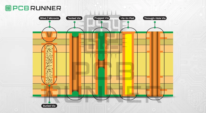
What is a Via?
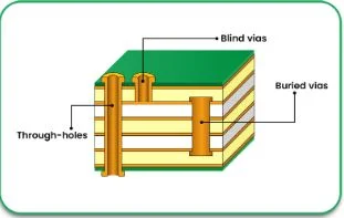
A via is a hole in the PCB filled or plated with copper. It lets current travel between different layers of the board. There are three main types:
- Through-hole vias – go from top to bottom of the board
- Blind vias – connect outer layer to inner layer
- Buried vias – connect inner layers only
Each one helps the current move through the board. But not all vias can carry the same current carrying capacity.
Why Via Current Matters
Just like traces, vias have limits. If too much current flows through a via, it heats up. That heat can damage your board, melt the copper, or cause cracks over time. You need to make sure your via can carry the right amount of current for your circuit.
If you’re working with printed circuit board manufacturers, ask them to help calculate this during the design process.
Understanding PCB Current Carrying Capacity
Before we look at vias specifically, let’s understand the basics of PCB current carrying capacity. It’s the amount of current a copper trace or via can safely handle without overheating. This depends on a few things:
- Width and thickness of the copper
- Length of the trace or via
- Temperature rise allowed
- Whether it’s on the outer or inner layer
You can use a PCB current carrying capacity calculator to help figure this out. It gives you a rough idea based on your design choices.
How Via Size Affects Current
The via size is key. Larger diameter vias can carry more current. Smaller vias carry less. You also need to look at how thick the copper plating is inside the via.
A common rule: A via with 1 oz copper plating and 0.3 mm diameter can carry around 1 amp with safe temperature rise. But this is just a guideline. Always double-check with a PCB trace current carrying capacity calculator or your PCB board manufacturer.
Learnt About: How to Accurately Calculate PCB Trace Width
Ways to Improve Via Current Carrying Capacity
If your via needs to carry more current, here are some options:
1. Use Larger Vias
A bigger hole means more copper and less resistance. This can carry more current safely.
2. Use Multiple Vias
Instead of one large via, use several smaller ones in parallel. This spreads the current and reduces heat.
3. Increase Copper Plating
Ask your PCB manufacturer for heavier copper plating inside the via. This lets more current pass through.
4. Use Via-in-Pad
This method puts the via directly in the pad under a surface-mounted part. It saves space and helps with heat transfer too.
Real Example: Power Supply Board
Let’s say you’re making a power supply board. Some traces carry 5 amps or more. If the vias between layers are too small, they could fail fast.
In this case, you’d:
- Use 3-4 vias in parallel
- Make each via at least 0.5 mm wide
- Ask for 2 oz copper plating
That helps spread the current and keeps the board safe. Your design works better, and you avoid future failures.
Choosing the Right Via for Your Design
When you plan your PCB, ask yourself:
- How much current will pass through each via?
- How many layers does my board have?
- Is my current mostly DC or AC?
- Do I need thermal relief?
These answers help you pick the right via size and layout.
If you’re not sure, your PCB circuit board manufacturer can help you figure it out. Always share your full design and ask for feedback.
Tools That Can Help You
Here are a few tools you can use during design:
- PCB trace width calculator – helps with trace sizing
- PCB current carrying capacity calculator – tells you how much current your trace or via can handle
- Track width calculator – similar to trace width calculator, focused on track layout
These calculators let you test different values before sending your design for production.
Talking to Your Manufacturer
Always talk to your PCB board manufacturer early in the process. Share your:
- Expected current levels
- Temperature limits
- Layout files
- Layer count
The more info they have, the better they can guide you. Some PCB circuit board manufacturers offer free design review to check for weak spots in current handling.
Common Mistakes to Avoid
Here are some things to watch out for when designing for via current:
- Using just one small via for high current
- Forgetting to match the trace and via size
- Ignoring temperature rise
- Not testing your layout with a calculator
Fixing these mistakes early saves money and time later.
When to Use Custom Solutions
If you’re building something special like a custom printed circuit board, your current needs might be higher than usual. In this case, you may need:
- Heavier copper boards (2 oz or more)
- Filled vias (for better thermal and current performance)
- Special via types like microvias
Talk to printed circuit board manufacturers that offer these services. Make sure they understand your design goals.
Final Thoughts
Vias are small, but they play a big role in your PCB’s performance. If they can’t carry enough current, your board might heat up, break down, or fail altogether. By choosing the right via size, using multiple vias, and checking with a PCB current carrying capacity calculator, you can keep your design safe and reliable.
Always put time into planning your via layout. Use tools. Talk to your pcb board manufacturer. And remember, every amp matters when you’re designing for long-term success.

