Designing custom printed circuit boards for today’s compact, high-speed electronics requires more than just traditional surface mountain. Engineers face shrinking form factors, heat management challenges, and signal-integrity issues. Embedding components inside the board itself addresses these constraints.
The printed circuit boards are the brains of any modern device. When designing or fabricating a custom printed circuit board, integrating components into the board can be more efficient with regard to area, performance, and reliability.
This blog outlines the techniques of embedding components into PCBs.
Methods of Integrating embedded components into printed circuit boards
Printed circuit boards traditionally mount parts on the surface. But embedding changes the game. In a custom printed circuit board or DI printed circuit board, passive parts and even ICs can be laminated inside the stack.
Embedding:
- Enhances the complexity of the design and the density of the layout without enlarging the board.
- Shields components from mechanical wear, dust, and damage.
- Shortens signal pats, improving accuracy and speed.
- Enables the development of lighter, smaller, and more reliable devices.
The trend of miniaturization is more noticeable with advanced printed circuit boards, like HDI printed circuit boards or specialized ones.

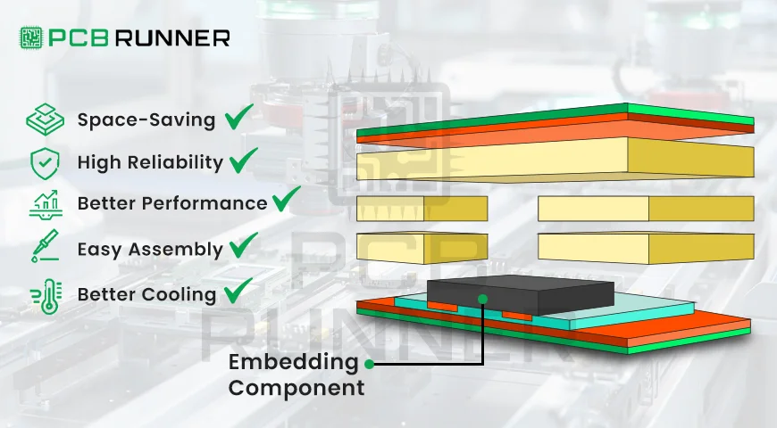
Benefits of Embedding Components
The advantages of embedding components on a circuit board are the following:
- Space Saving: Embedding either increases the surface area within the circuit board for the addition of other parts or reduces the surface area of the PCB overall. This is crucial for wearable electronics.
- Enhanced electrical performance: Internal component placement reduces parasitic effects as well as signal interference when compared to external component mounting. This increases accuracy and speed.
- Greater reliability: Parts that are embedded are more reliable when it comes to protecting against mechanical shocks, dust, or corrosion.
- Reduced soldering steps: Embedding cuts the number of solder joints and placements, lowering assembly errors and shortening production time.
- Some embedded approaches enhance the dissipation of heat, which improves thermal management.
At pcbrunner, we specialize in PCB embedding solutions that bring all these advantages into your design.
Key Approaches to Embedding Components in PCBs
There are other approaches to the embedding of components in printed circuit boards, other than the component placement:
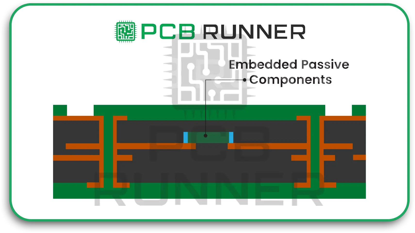
Creating Cavities or Slots in PCB Layers
This approach is cavity embedding:
The precision cavity approach involves the machining or laser drilling of the recesses into the PCB layer. This technique is often referred to as cavity embedding.
Chips or components are placed into the recesses so that they are flush or below the layer surface.
The parts are secured to the recesses using adhesives.
Subsequent layers of prepreg or a core layer are added to the initial layers to seal and build the stacked PCB.
This technique is mainly applied in the embedding of passive components such as resistors and capacitors, as well as thin IC packages. They enable better integration without the addition of surface board thickness.
2. Sandwiching Parts Between Prepreg Layers
Prepreg materials are crucial in PCB lamination. Manufacturers:
* Position components between sheets of prepreg (semi-cured resin sheets).
* Stack several prepreg and core layers containing parts within them.
* Heat and apply pressure to cure the stack to create a single, solid, bonded piece.
This method effectively incorporates both active and passive components. It is essential to control material thickness to avoid warping the board.
3. Via Connections and Laser Drilling
The rest of the board requires electrically connecting the embedded parts. Laser micro-drilled vias do the following:
* Drilled access holes to reach pads on the embedded components.
* Currently used to conduct the vias with copper electrically.
* Attach embedded components directly and eliminate the need for long traces.
This is especially important in HDI printed circuit boards for the backbone of connecting hidden components in restricted spaces using laser via technology.
4. Embedding with Film
Thin substrate materials are transformed into flexible ones using:
* Thin polymer films are used to place components on.
* Films are then incorporated into multilayer PCBs.
This is important for flexible and bendable PCBs where there are no rigid cavities.
5. Additive and 3D Printing Techniques (Emerging)
A few manufacturers are looking into 3D printing and additive manufacturing for embedding:
The addition and layering of particular conductive and insulating materials.
There are mid-process component integrations.
While they are still in the experimental phase, this could enable incorporating more intricate designs with different geometries.
Prototyping Considerations for PCB Prototypes with Embedded Components
Before moving to mass production, it’s a smart idea to build at least one PCB prototype with the planned embedded components. Working closely with your PCB supplier early on helps you to understand key process limits like how deep cavities can go, the tolerances for laser-drilled vias, and the thickness of prepreg materials. By adjusting your design to fit within these limits, you can avoid expensive rework later and get your product to market faster.If you’d like expert support with prototyping or need clarity on design tolerances, our team is here to guide you through every step before mass production to contact our sales engineer contact us today at sales@pcbrunner.com.
Tips for Designing with Embedded Components –
Get the order right for cavity and embedded components placement: The PCB thickness and spacings between layers to be mounted must be considered.
- Don’t overly restrict space for routing: Space for routing and connections must be available for laser-drilled fine vias.
- Consult with the suppliers: Component embedding feasibility can be confirmed with suppliers.
- Respect weak zone distances: Minimum distances around embedded components are short, weak zones, or damaging structural integrity.
What are the Impacts of Embedding on the PCB Fabrication and Assembly Processes?
The addition of components that embed firmly changes the entire PCB production life cycle:
- Fabrication complexity: undergoes changes with layering precision, requires specialized equipment (laser drills), and careful pre-cured board stacking for uniform board thickness.
- Blind and active inspection: embedded components require specialized X-ray inspection methods for verification of placement and connection for the part hidden in the layers.
- Assembly: the surface-mount assembly stage is less. But requires high-level precision in PCB layout to ensure that all embedded components interface appropriately with via nets. Embedded components must withstand the temperature and pressure of lamination.
- Cost: Embedding parts increases the cost. But, in most cases, production cost and time are reduced, and the entire system size and intricacy are increased.
HDI Printed Circuit Boards and Embedding
Mobile and aerospace industries utilize HDI (High Density Interconnection) PCBs. They are embedding-enhanced for increased efficiency:
- Incorporating passive components into HDI stackups helps to reduce the number of board layers.
- Permits the use of small microvias and laser-etched cavities to densely pack functions.
- Increases signal integrity and improves reliability for high-speed designs.
Conclusion
Integrating components into printed circuit boards eliminates several steps in the processes of miniaturizing and accelerating the efficiency of electronic devices. Manufacturers are able to make custom printed circuit boards and HDI printed circuit boards using advanced techniques like cavity creation, prepreg lamination, and laser via truly remarkable connections.
Whether you are designing a PCB prototype or strategizing for large-scale production to know how embedding techniques interact with circuit board components. For further guidance, reach out to PCB Runner.

