Achieving the utmost performance in high-speed PCB design requires steady signal integrity while minimizing losses. One prominent evaluation measure is the Channel Operating Margin (COM) because it gives an approximate understanding of how robust a system is to high-speed data throughput.
The progress of high-density interconnect (HDI) technology is constantly pushing the boundaries of printed circuit boards via trace design. So, COM analysis can also be very beneficial in enhancing the reliability and efficiency of the PCBs.
Understanding Channel Operating Margin (COM)
COM is a high-speed communication channel figure-of-merit with respect to signal integrity. It quantifies how much noise, crosstalk, and various other factors might interfere before a signal becomes totally unreadable. Compared to traditional eye-diagram analysis, COM is way better since it takes a more holistic, simulation-based approach to evaluating PCB performance.
Some of the factors that affect COM include:
Losses in PCB traces and vias: The trace signal amplitude will be attenuated due to high-speed signal travel through the PCB materials.
Crosstalk from adjacent traces: Denser circuitry can result in inter-component interference.
Reflection and impedance mismatches: Vias and trace terminations that have not been well optimized can result in underperformance.
Improving COM Scores with COM Analysis in High-Speed PCB Design
PCB Position for Optimized Signal Integrity
A laid-out PCB, which is optimized, should enhance the Channel Operating Margin. Appropriate placement of the signal traces, as well as the power and ground plane, should be kept clear of interference and power loss. High-density interconnect (HDI) technology enables finer trace throughput and reduced signal path lengths, therefore increasing COM scores.
Choosing the Correct PCB Components
The component selection process is critical in high-speed PCB design. Using low-loss dielectric materials with controlled impedance characteristics helps mitigate signal degradation. Furthermore, high thermal stability sub-laminates should be focused on to ensure performance is maintained during operational conditions.
Improving Via Construction
The design of printed circuit board vias is challenging to achieve signal integrity for high-speed applications. Conventional through-hole vias cause discontinuities that lead to self-reflections and signal attenuation. To reduce the effects of this, the engineer should:
* Use blind and buried vias in order to reduce stub length on the vias.
* Use back-drilled vias to get rid of signal reflections.
* Change the pad size of the via for better-controlled impedance.
A COM analysis uses simulation to estimate the potential performance of a PCB before the actual fabrication of the board. Engineers can model design parameters like trace routing via placement and materials selection to simulation tools. Time-domain reflectometry (TDR) and vector network analysis (VNA) are employed post-manufacture to verify that the device functions as intended.
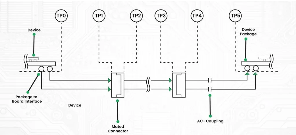
Utilization of Channel Operating Margin in PCB Layouts
An important factor in the performance assessment relating to the channels configured on the PCB is the evaluation of high-speed electrical channels. The two data pins of the IC and the two pluggable connectors on the edge of the PCB form a critical high-speed data path. Various factors influence the quality of the signals on these high-speed data links:
- Track width
- The type of PCB dielectric
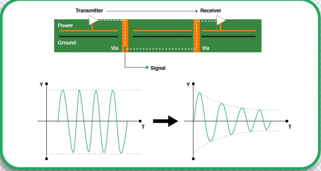
- Discontinuities over the track and component pads that can cause reflections
- Track length and type: stripline vs microstrip
- The physical configuration of vias
- Dependency of signal quality, such as jitter on data pattern
- Temperature dependency
As frequency increases, track dimensions and PCB dielectric properties tend to dominate. An electromagnetic wave in a dielectric material moves with a velocity proportional to the inverse of the square root of the dielectric constant. An increase in the dielectric constant results in a decrease in wave velocity, which in turn affects signal transmission.
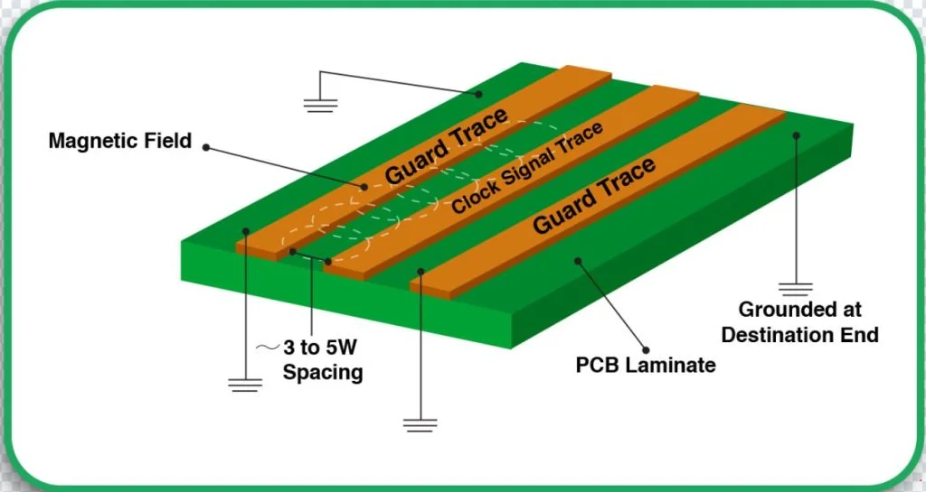
Aside from dielectric absorption, losses associated with transmission also accrue due to the skin effect. The skin effect restricts the flow of electric current to the outer surface of the conductor; hence, widening copper traces may help reduce it. However, at higher frequencies, the losses incurred due to the dielectric material are predominant over the losses incurred due to the skin effect. Because of that, the selection of the dielectric material for PCBs operating at frequencies greater than 5 GHz becomes very important.
In order to meet the requirements of higher speeds, Channel Operating Margin (COM) is used as a metric for assessment. COM is a parameter used for high-speed PCB design and enables design assessment of systems that go beyond 25 Gbps. The metric assesses the interactions of the transmitter, channel, and receiver, emitting a value in dB, which expresses the strength of the design. Any design which exceeds a COM figure of 3 dB is considered valid. The analysis of COM allows designers to ensure the design complies with criteria while preventing overdesign.
Expert Insight
The rapid growth in the data rates, as well as the new modulation techniques being developed in various telecom standards, is the reason why high-speed serial link design is growing in popularity in the electronics sector. It is also possible that traditional certification metrics are problematic and may cause sub-optimal transmit (Tx) and receive (Rx) circuit designs. Consequently, the Ethernet standard IEEE 802.3bj defined a different COM that lets the user examine the design space at an early stage, which is much simpler. Without reports on the application of COM as an adjunct design method on circuits of transceivers, some works explore its potential as a backplane design tool.
This study investigates the use of COM as a complementary metric for transceiver circuits, such as the COM performance for four 100GBASE-KP4 backplanes with different equalization architectures. The metric is evaluated while cognizant of the impact and challenges associated with the incorporation of novel equalization structures into the flow of COM. A conventional architecture discovered by the focus group has been found to dominate the COM metric when applying the Tx-Rx cutoff architecture. The Tx-Rx cutoff architecture results in a significantly better opening of the eye diagram but does not satisfy the cutoff threshold.
Conclusion
The question of high-speed PCB design is now more paramount than ever, particularly due to the rapid increase in data rates. If engineers integrate Channel Operating Margin (COM) analysis into the development stage, they can improve signal integrity, decrease signal losses, and increase overall system reliability. Achieving optimal PCB performance requires the integration of advanced interconnect technologies and the refinement of printed circuit board vias.
Are you looking to improve your PCB design with superior COM analysis? Contact PCB Runners today to find out how our high-speed PCB design services can boost the success of your next project.

