In the evolving world of custom printed circuit board manufacturing, precision is everything. As data speeds increase and electronic devices become more compact, signal quality and consistency become paramount. One key factor behind reliable high-speed data transmission is defined impedance a controlled value that ensures signals travel through PCB traces without unwanted reflections or distortions.
For every pcb manufacturer in Europe or globally, maintaining defined impedance isn’t just a design choice; it’s a necessity for achieving stable PCB signal integrity and long-term reliability.
Why Defined Impedance Matters in Modern High-Speed PCBs
With the rise of high-speed PCB design, electronic systems today must support gigabit data rates, differential signaling, and complex multi-layer structures. Impedance control ensures each transmission line (trace) behaves predictably, preventing reflections that cause signal degradation or timing errors.
Defined impedance directly affects PCB performance optimization — an incorrectly matched impedance can reduce signal amplitude, introduce noise, and even cause complete data loss. Whether in automotive radar, 5G modules, or aerospace control systems, stable impedance enables consistent performance across temperature, voltage, and manufacturing variations.
For a custom printed circuit board, impedance definition typically falls between 50Ω (single-ended) and 90Ω (differential). Achieving this consistency requires precise control over dielectric materials, copper thickness, and trace geometry.
Fundamentals of Impedance, Transmission Lines & Signal Integrity
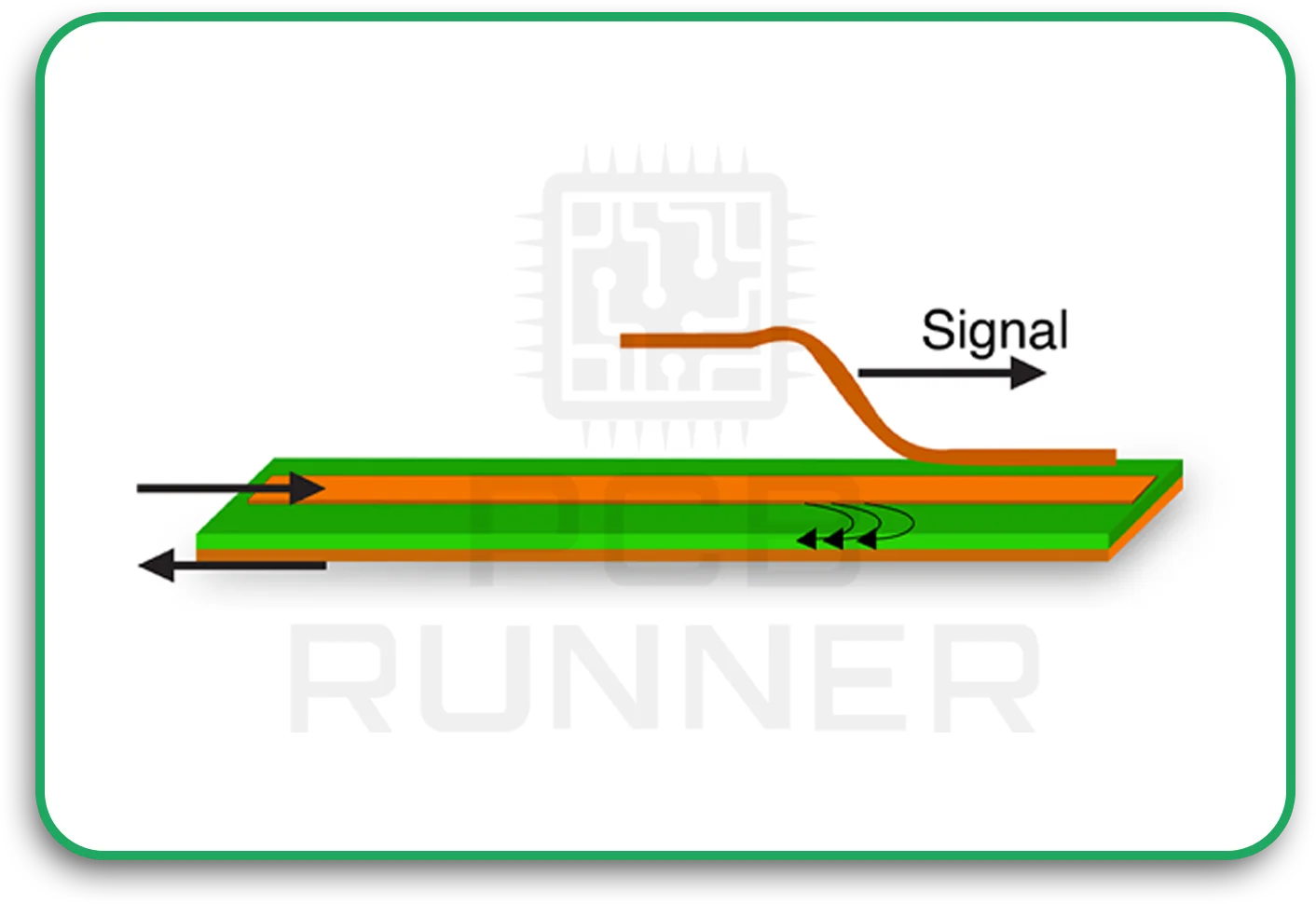
Understanding impedance is essential before mastering high-speed PCB design. Impedance is the opposition that a circuit presents to alternating current — in PCBs, it depends on trace width, height above the reference plane, and the dielectric constant of the substrate.
Signal reflections, return loss, and mismatch effects
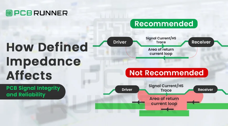
When the impedance of a transmission line doesn’t match the load, part of the signal reflects back toward the source, degrading PCB signal integrity. These reflections cause return loss and can distort digital waveforms, leading to data errors.
In high-speed environments, even small mismatches can create ringing, crosstalk, or EMI issues. Maintaining consistent impedance throughout the signal path helps avoid these reliability problems.
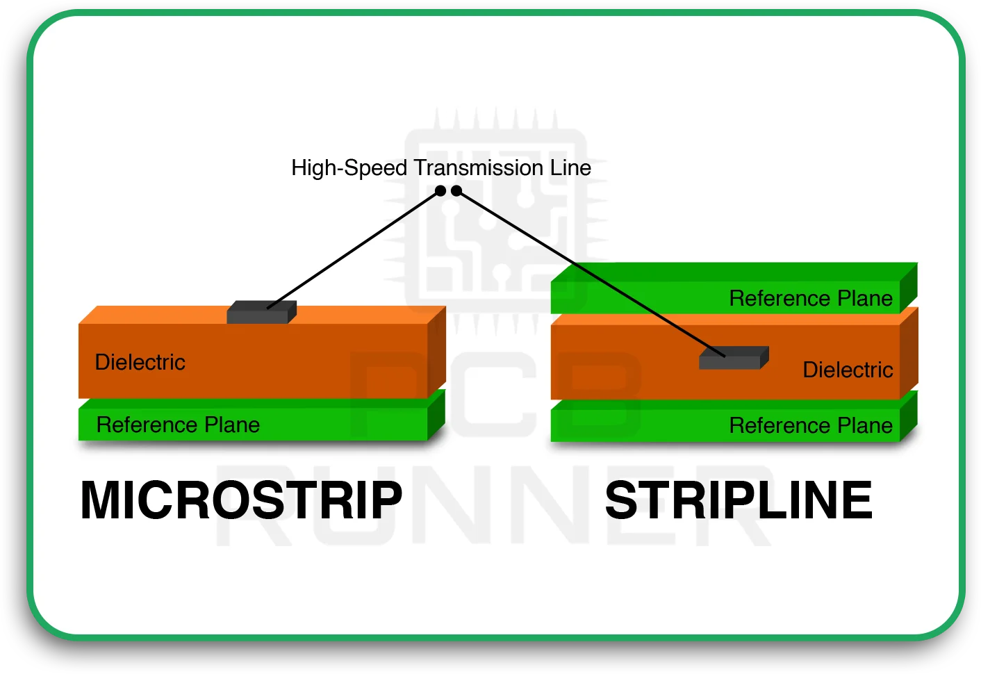
Microstrip, stripline & differential pair characteristic impedance
Different routing methods influence impedance control.
- Microstrip lines (traces on the outer layer) have one reference plane beneath them.
- Striplines (internal layers) have two reference planes and offer better shielding.
- Differential pairs use two coupled traces to carry complementary signals, with an impedance typically set to 90Ω.
Selecting the right configuration is key to balancing manufacturability, cost, and PCB performance optimization.
Designing for Defined Impedance in High-Speed PCB Layouts
The layout stage is where most impedance-related issues can be prevented. During custom printed circuit board design, engineers define trace widths, spacings, and layer stack-ups based on the target impedance.
Stack-up, dielectric constant, trace geometry considerations
The PCB stack-up determines how signals travel between layers. The dielectric constant (Dk) of the material affects signal propagation speed — variations in Dk can cause impedance drift. To ensure stable impedance, designers must use controlled dielectric materials and consistent copper thicknesses.
Modern pcb manufacturers in Europe provide online impedance calculators and stack-up design tools that let engineers simulate impedance before fabrication, ensuring accuracy and predictability.
Via transitions, layer changes, and impedance discontinuities
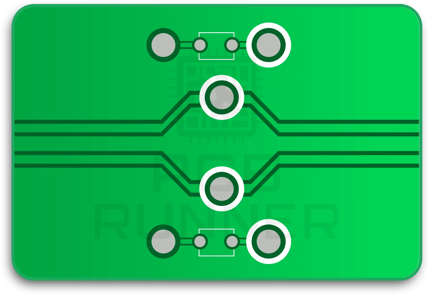
Each via or layer transition can alter the signal path’s geometry, introducing impedance discontinuities. Proper design — using backdrilled vias, anti-pads, or via stubs — minimizes these variations. Maintaining smooth transitions helps preserve PCB signal integrity, especially in differential pairs used for USB, HDMI, or PCIe signals.
Manufacturing and Verification: Ensuring Impedance Accuracy
Even the best design can fail if manufacturing doesn’t maintain the specified impedance. That’s why collaboration between designers and a pcb manufacturer in Europe or trusted fabrication partner is crucial.
Coupon, TDR, and VNA testing methods
During production, custom printed circuit boards often include test coupons — miniature replicas of signal traces — to verify impedance consistency. Manufacturers use Time Domain Reflectometry (TDR) or Vector Network Analyzer (VNA) testing to measure actual impedance and detect mismatches.
Tolerances, process control, and design-to-manufacturing alignment
Impedance tolerances are typically ±10%. Maintaining them requires tight process control over etching, plating, and lamination. European PCB suppliers emphasize process repeatability and material traceability to ensure high-speed PCB design reliability at scale.
Partnering early with your manufacturer ensures your custom printed circuit board design parameters align with real-world fabrication capabilities — the hallmark of effective PCB performance optimization.
Implications for Reliability & Long-Term PCB Performance
Stable impedance directly enhances long-term PCB signal integrity and reliability. Mismatched impedance leads to localized heating, bit errors, and premature aging of components.
When designed and verified correctly, defined impedance reduces jitter, improves timing margins, and allows faster data rates without increasing error rates. In harsh environments like aerospace or industrial systems, this translates to consistent performance even under temperature or vibration stress.
For designers, that means fewer redesigns and better end-product reliability. For any pcb manufacturer in Europe, it demonstrates technical expertise and manufacturing precision — key differentiators in the global electronics market.
Partnering with a Trusted PCB Manufacturer for Defined Impedance Control
The effectiveness of impedance control lies not only in design tools but also in collaboration. A custom printed circuit board partner who understands the nuances of high-speed PCB design can help optimize layer stacks, select materials, and test impedance during every stage of production.
Choosing a reputable pcb manufacturer in Europe ensures compliance with IPC standards, consistent process control, and transparent quality assurance — vital for maintaining signal reliability in today’s complex electronics.
Conclusion: Defined Impedance — The Cornerstone of PCB Reliability
Defined impedance isn’t just a technical parameter; it’s the foundation of reliable signal transmission and consistent performance in modern electronics. Whether you’re designing for automotive, telecom, or industrial systems, integrating impedance control during the custom printed circuit board design phase is essential for PCB performance optimization.
By working closely with an experienced pcb manufacturer in Europe, you can ensure that your design intent translates accurately to production — resulting in superior PCB signal integrity, enhanced durability, and products built for the future of high-speed communication.

