Ever wondered why some circuit boards last for years, while others fail in months? The answer often lies in the details, especially in how the board is designed and built. One of the most essential details is clearance. That’s the space between different parts of your PCB. Get it right, and your board works safely and reliably. Get it wrong, and you risk short circuits, noise, or even total failure.
Let’s explore how printed circuit board manufacturers, circuit board suppliers in the UK, and design teams utilise clearance strategies to create high-performance PCBs that stand the test of time.
Why Clearance Matters in Circuit Board Design
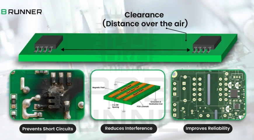
Clearance is more than just empty space. It’s a shield, protecting your board from electrical problems, heat, and even physical damage. In circuit board design, clearance means the minimum distance between copper traces, pads, and other conductive elements.
Why is this important?
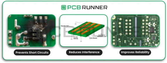
- Prevents short circuits: If traces are too close, electricity can jump across and cause a short.
- Reduces interference: Proper spacing helps avoid signal noise and crosstalk.
- Improves reliability: Boards with good clearance are less likely to fail, even in harsh environments.
Think of clearance like the lanes on a motorway. If cars (signals) have enough space, traffic flows smoothly. If lanes are too narrow, accidents are more likely to occur.
Key Clearance Strategies for High-Performance PCBs
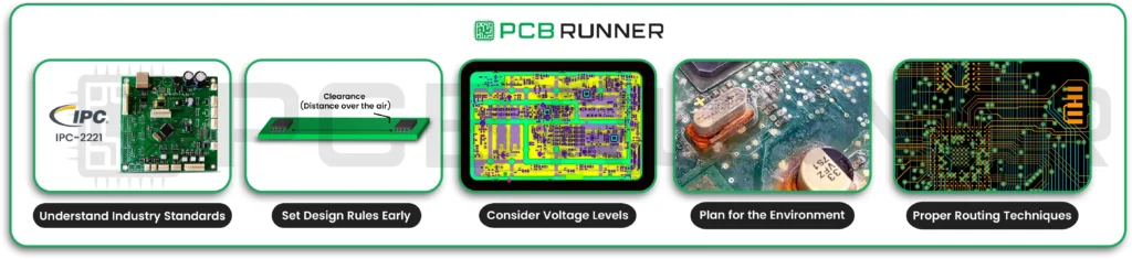
1. Understand Industry Standards
Most PCB board manufacturers follow strict rules set by groups like IPC. For example, IPC-2221 provides guidelines for minimum spacing based on voltage and environmental conditions. Always verify the standards your project requires.
2. Set Design Rules Early
Before you start your PCB layout, set your clearance rules in your design software. This helps avoid mistakes later. Good PCB manufacturing services will review these rules before production begins.
3. Consider Voltage Levels
Higher voltages need more space between conductors. For example, a board handling 1000V needs much bigger gaps than one with 5V signals. This helps prevent arcing and breakdown.
4. Plan for the Environment
Boards exposed to moisture, dust, or chemicals need extra clearance. Contaminants can lower the breakdown voltage, making shorts more likely to occur. Outdoor or industrial boards often need wider gaps than those used in clean offices.
5. Use Proper Routing Techniques
- Keep traces apart: Space traces generously to avoid crosstalk and interference.
- Avoid parallel runs: Don’t run high-speed or high-voltage traces side by side for long distances. If you must cross, do it at right angles.
- Solid ground planes: Use large, continuous ground planes to shield signals and improve stability.
The PCB Layout Process: Step by Step
Designing a reliable PCB isn’t just about drawing lines. It’s a careful process that involves planning, checking, and testing at every stage.
Step 1: Define Your Goals
Begin by determining what your board needs to accomplish. Make a list of features, connections, and size limits. Think about where the board will be used. Will it be exposed to high temperatures, vibration, or moisture?
Step 2: Create a Schematic
Draw a detailed circuit diagram. This is your blueprint, showing every part and connection. A clear schematic makes the next steps much easier.
Step 3: Choose Components and Place Them Wisely
Place parts based on their function, heat resistance, and accessibility. Group related parts together. Keep high-power and sensitive parts apart. This makes routing easier and reduces interference.
Step 4: Route Traces with Clearance in Mind
Connect the parts using traces. Follow your clearance rules. Use wider traces for high current. Add extra space around high-voltage areas. If you need to change layers, use multiple vias for heavy currents.
Step 5: Review, Test, and Validate
Check your design for errors. Use your software’s design rule check (DRC) to catch spacing problems. Build a prototype and run tests for continuity, resistance, and capacitance. Fix any issues before moving to mass production.
High-Voltage Clearance: Safety First
If your board handles high voltages, like in electric vehicles or industrial machines, clearance becomes even more critical. Here’s what to keep in mind:
- Clearance: This is the shortest distance through air between two conductors.
- Creepage: This is the shortest path along the surface of the board.
Both must be large enough to prevent arcing or breakdown. Always follow industry standards and consult with your PCB fabrication assembly partner if unsure.
Do:
- Use your design tool’s DRC to enforce spacing rules.
- Create special “high voltage” zones with extra clearance.
- Double-check spacing visually and with your manufacturer to ensure accuracy.
Don’t:
- Rely on default spacing for high-voltage areas.
- Route high-voltage traces under components that have insufficient space.
- Ignore the effects of dust, moisture, or ageing on insulation.
Tips for Different Board Types and Applications
Every project is different. Here are some tips for everyday situations:
For consumer electronics:
- Space is tight, but don’t skimp on clearance.
- Use ground planes to reduce noise.
- Keep power and signal traces apart.
For industrial or outdoor boards:
- Use wider gaps to handle dirt, moisture, and higher voltages.
- Protect traces with conformal coating if needed.
For high-speed boards:
- Avoid long parallel traces.
- Use controlled impedance traces where needed.
- Keep return paths short and direct.
For multi-layer boards:
- Use internal layers for power and ground.
- Stagger the vias to avoid bottlenecks.
Lesson: Always design with the real world in mind, not just the clean lab.
How Circuit Board Suppliers UK Help with Clearance
Good circuit board suppliers in the UK and PCB board manufacturers do more than just build boards. They review your design, check for clearance issues, and suggest improvements. Some even offer after-sales support and quick assistance if you encounter any problems.
Choosing a supplier with experience in your field, whether it’s medical, aerospace, or industrial, means they know the common pitfalls and how to avoid them.
Product Highlights: What to Look for in PCB Manufacturing Services
When choosing a PCB manufacturing services partner, look for:
- Experience with your application: Medical, automotive, industrial, etc.
- Clear communication: They should explain their clearance and quality checks.
- Fast prototyping: Quick turnarounds enable you to test and refine your design.
- Quality certifications, including ISO 9001 and IPC standards, demonstrate a commitment to quality.
Final Thoughts: Small Gaps, Big Impact
Clearance might seem like a small detail, but it’s one of the most essential parts of circuit board manufacturing. With the right strategies, you can build boards that work reliably, even in harsh conditions. Whether you’re a hobbyist, engineer, or buyer, understanding clearance helps you make better choices and avoid costly mistakes.
So next time you sit down to design a PCB, remember: a little extra space can make all the difference. Give your signals room to breathe, and your board will appreciate it.
Designing high-performance PCBs isn’t just about clever circuits or fancy parts. It’s about getting the basics right, starting with clearance. Keep it simple, keep it safe, and your boards will deliver top performance every time.

