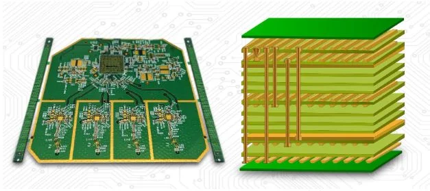
The design of a High-Density Interconnect (HDI) PCB is essential today due to the evermore shrinking and demanding electronic parts. The complex structure of an HDI PCB, along with its unique fabrication techniques, helps PCB manufacturers fulfill the needs for increasingly smaller and more powerful devices.
As with most design work, one of the most important parts of it is assembling the correct stack up. This blog will discuss various stackup configurations and how to select the most appropriate one.
What is an HDI PCB Stackup?
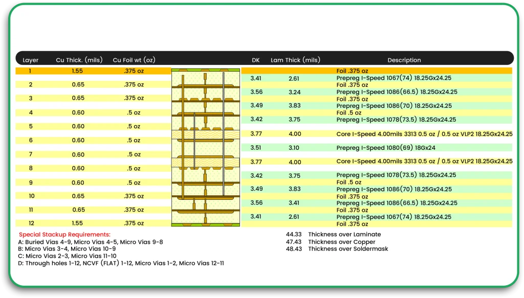
An HDI PCB stackup is the configuration of the conductive and non-conductive layers of a printed circuit board patterned out on the PCB. It decides the ordering of signal routing, power distribution, and the mechanical and electrical operations of the entire board.
Optimize stackup design approaches to ensure the reliability of signals, reduction of electromagnetic interference (EMI), and improve overall strength of the PCB.
Why is Stackup Selection Essential?
Choosing the correct stackup is fundamental to maintaining the power distribution while ensuring signal integrity in an HDI PCB design. Signal loss, boosted level of crosstalk, and more challenging procedures during fabrication can all stem from poorly assembled stackups.
Key factors influenced by the stackup include:
Routing Density: Efficient use of layers can support complex routing paths.
Signal Integrity: Proper stackup reduces noise and interference.
Cost Efficiency: The number of layers and types of vias affect manufacturing costs.
Common HDI PCB Stackup Types
Most PCB companies use the following three stackup types for HDI PCBs.
1. Standard Lamination with Vias or Plated Through Holes (PTHs)
This type of stackup uses a simple lamination process with traditional through-hole vias connecting all layers.
Advantages:
- Cost-effective for designs with fewer layers (28 layers or less).
- Simplifies the manufacturing process.
Disadvantages:
- Limited routing capabilities for complex designs.
- Not suitable for high pin-count Ball Grid Arrays (BGAs) with pitches below 0.8 mm.
- Challenging to manage high-density signal paths.
2. Sequential Lamination with Plated Through, Blind, and Buried Vias
This configuration includes blind and buried vias in addition to through vias.
Advantages:
- Improved routing capabilities compared to standard lamination.
- Reduced via stubs and smaller via diameters.
Disadvantages:
- Higher fabrication costs.
- Limited practical layer count, typically up to three layers.
- Still less efficient for complex high-density interconnect applications.
3. Lamination Buildup with micro vias
This advanced stackup is especially suitable for high-density designs involving fine-pitch BGAs.
Advantages:
- Enables higher routing density with fewer layers.
- Smaller trace widths and via diameters.
- Better power and signal integrity.
- Cost-effective for high-frequency, high-density boards.
Disadvantages:
- Requires advanced manufacturing processes.
- Initially, it can be more expensive than traditional methods.
Benefits of Lamination Buildup with Microvias
Many leading HDI PCB manufacturers, including Rush PCB Inc., recommend lamination buildup with microvias for advanced high-density interconnect designs.
Why Choose Microvias?
- Higher Routing Density: Microvias allow designers to use fewer layers while achieving dense routing.
- Improved Signal Integrity: Smaller vias and shorter signal paths reduce interference and noise.
- Cost Efficiency: Despite initial costs, the reduced layer count and improved performance lower overall expenses.
- BGA Compatibility: Ideal for boards with multiple large BGAs with pitches below 0.8 mm.
IPC Standards for HDI PCB stackups
The IPC-2315 standard categorises HDI stackups into six types:
- Type I: Laminated core with a single microvia layer.
- Type II: Laminated core with microvias, blind, and buried vias.
- Type III: Laminated core with two or more microvia layers.
- Type IV, V, VI: More advanced and expensive configurations.
Let’s take a closer look at the most common types.
HDI Type I
- Structure: Laminated core with a single microvia layer.
- Vias: PTH and blind vias, but no buried vias.
- Use Case: Suitable for less complex high-density interconnect designs.
Limitations:
- The aspect ratio for PTH vias must be less than 10 for reliability.
- Thin FR-4 dielectrics may delaminate during lead-free soldering.
- It’s not ideal for large boards with multiple BGAs.
HDI Type II
- Structure: Laminated core with microvias, blind, and buried vias.
- Vias: Stacked or staggered microvias.
- Use Case: More suitable for complex designs than Type I.
Limitations:
- Outer layers are often restricted to power/ground planes.
- Less effective for single buildup layer routing.
HDI Type III
- Structure: Laminated core with two or more microvia layers.
- Vias: Stacked or staggered microvias, blind, and buried vias.
- Use Case: Best for complex, dense multilayer PCBs.
Advantages:
- Greater routing density.
- Outer layers are available for power/ground planes.
- Ideal for large boards with multiple BGAs.
Limitations:
- Higher fabrication costs.
- Still constrained by PTH and thin FR-4 dielectric limitations.
Choosing the Best HDI Stackup
When designing a HDI PCB, the following should be considered when selecting a stackup.
1. Demands of the Application
The complexity of the design, frequency of operation, and routing density should be examined in detail. The Type III stack-up is preferred for high-performing applications with dense routing.
2. Parts Choice
In cases where many fine-pitch BGAs are present, micro-via base stackups are preferred due to better routing.
3. Cost Constraints
Achieve performance targets without going over budget. Even though microvia stackups have a higher upfront cost, they are often the most cost-efficient in the long run due to fewer layers and better yield.
4. Signal Integrity and Power Distribution
Select the stackup that will optimise minimum interference. Lamination buildup with microvias is best for high-frequency applications.
Conclusion
The selection of the right stackup will greatly benefit your HDI PCB design. From the most basic design to a complicated board filled with fine-pitch BGAs, each stackup type has advantages and disadvantages that must be considered.
Working alongside a capable PCB manufacturer can aid in the choice of stack up, optimising the design and ensuring that industry requirements are met. Lamination buildup with microvias will always remain the best approach for HDI PCBs because of high routing density, good signal integrity, and low cost.
Choosing the right stackup, along with advancements in technology, will definitely increase a designer’s competitiveness in the field of high-density interconnect designs.
For such crucial information about PCB design, sign up to our updates at PCB Runners.

