Each PCB prototype project begins with a design idea; however, the success of that PCB often depends on something less obvious: the Bill of Materials (BOM). A properly-constructed BOM can be the difference between success and failure of production. For companies such as PCB Runner, maintaining an accurate and consistent BOM is essential for seamless PCB manufacturing and reliable results.
In the fast-moving European electronics industry, even a minor BOM error can delay production, increase costs, or cause an entire batch to fail quality inspection due to incorrect components. Knowing what could go wrong and how to avoid it helps engineers, designers and procurement teams develop better, more successful PCB workflows.
What Makes a Good BOM for PCB Projects
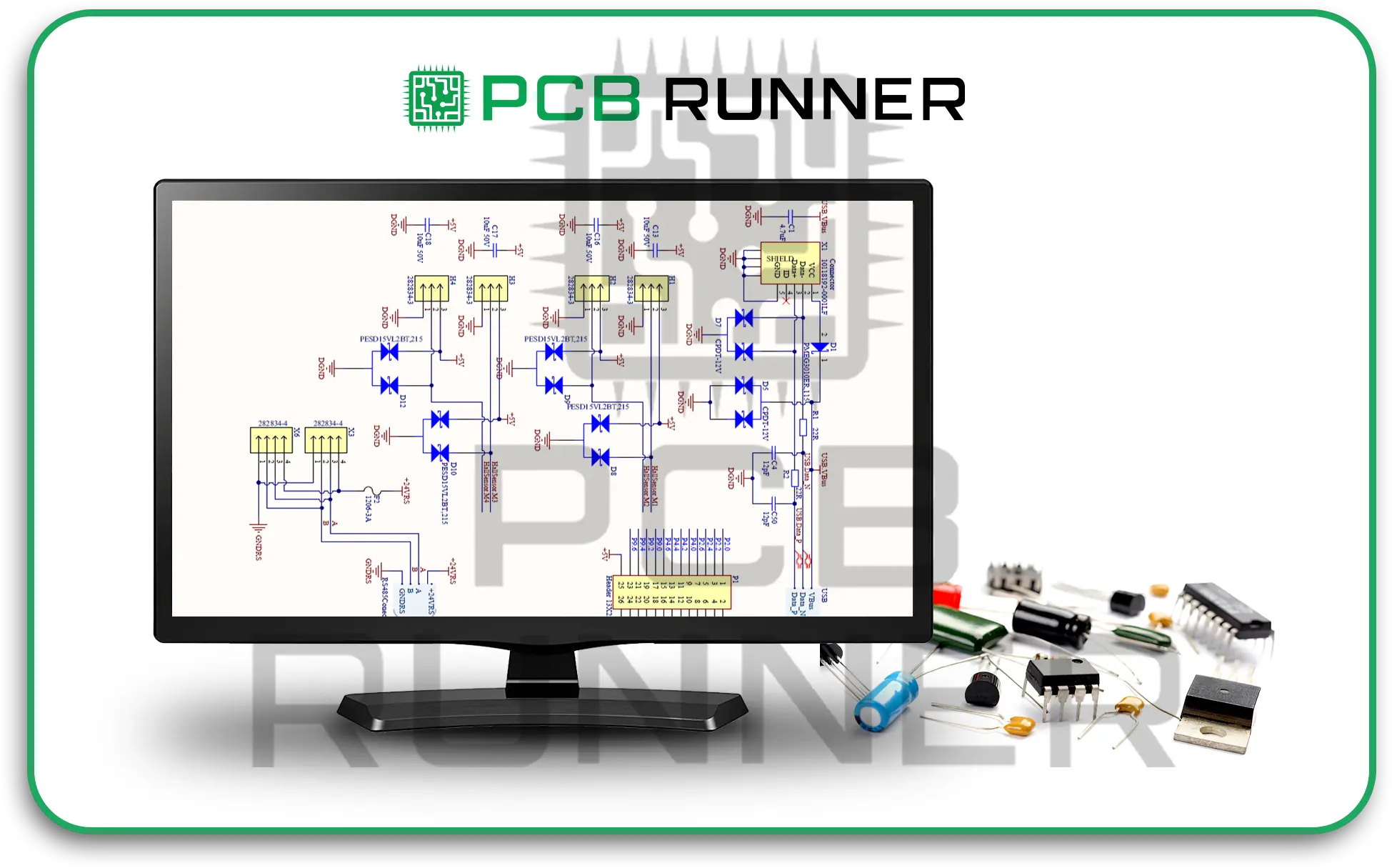
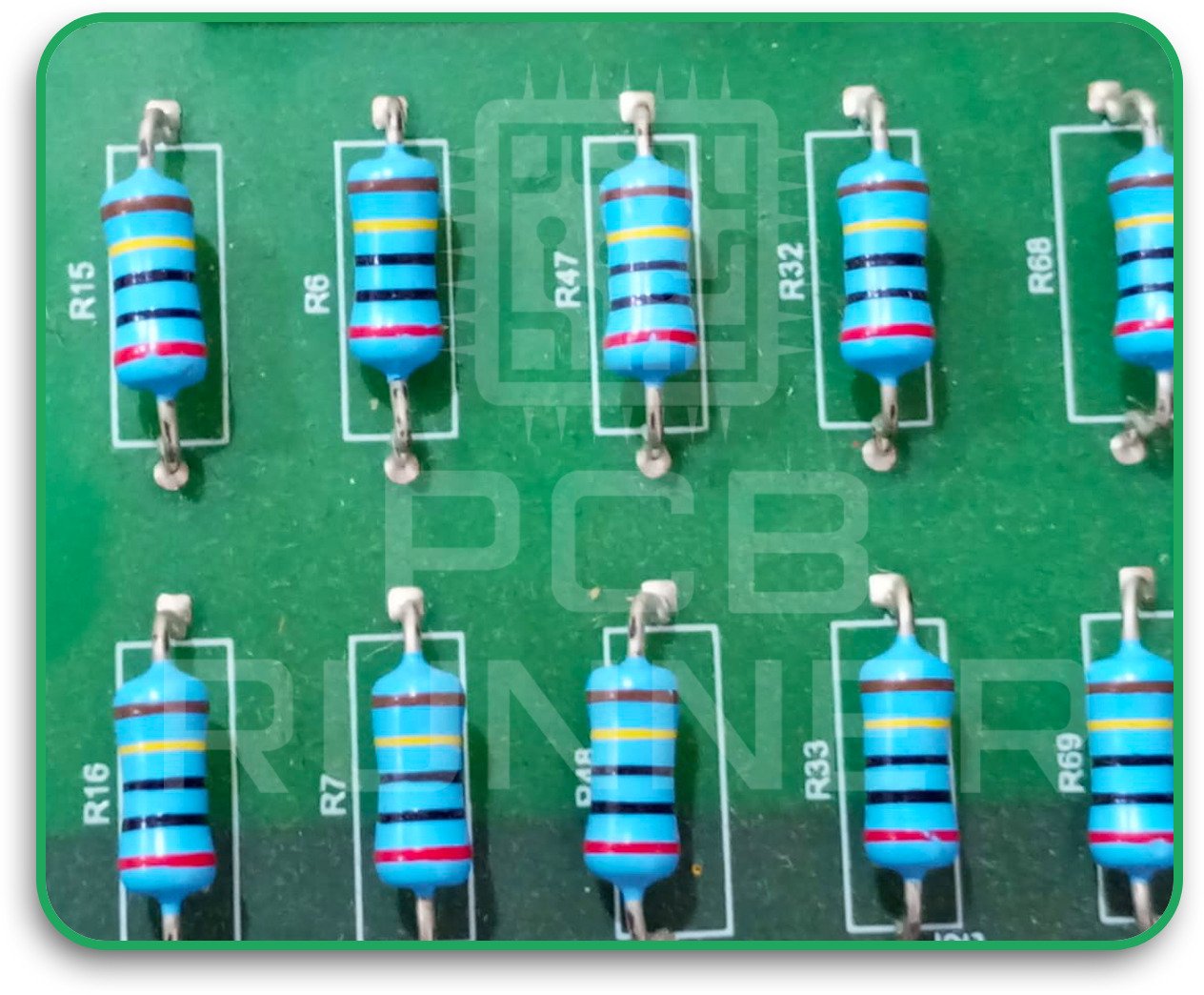
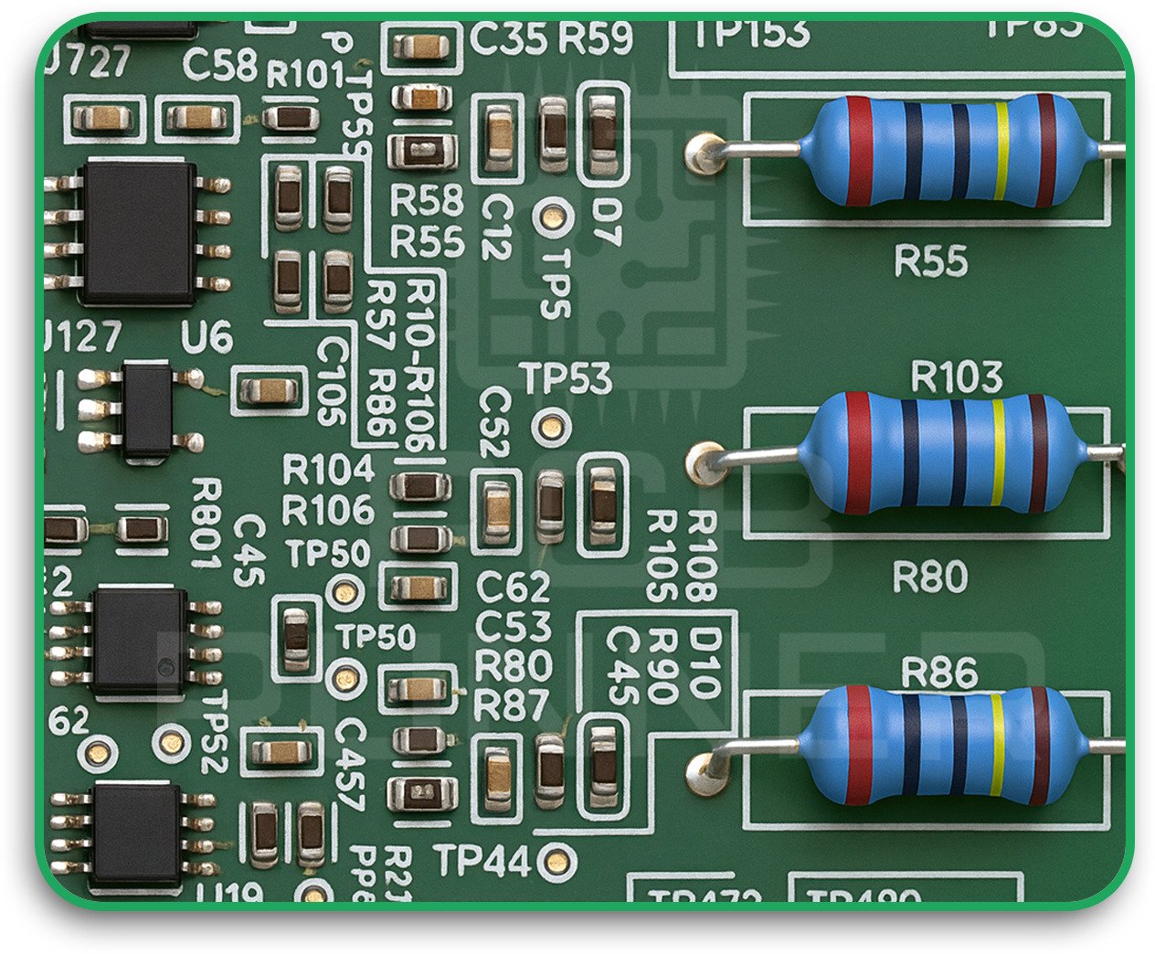
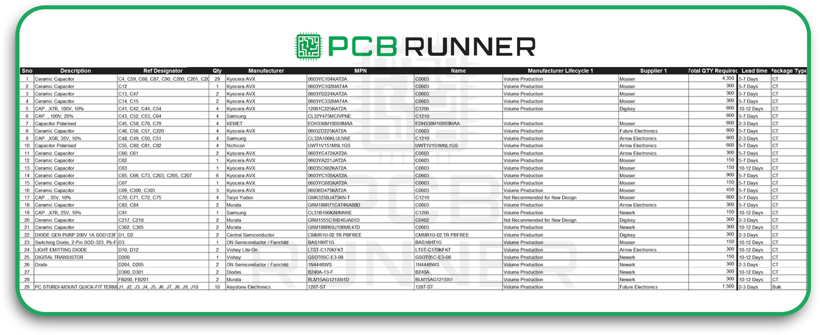
The BOM or Bill of Materials (BOM) is essentially the list of components of the PCB design. It lists every component within the circuit, including capacitors, resistors, connectors, and ICs, as well as small hardware pieces.
The purpose of the BOM is to provide PCB manufacturers with all the components they require to make the PCB the way they want it to be. The BOM bridges the gaps between design and manufacturing.
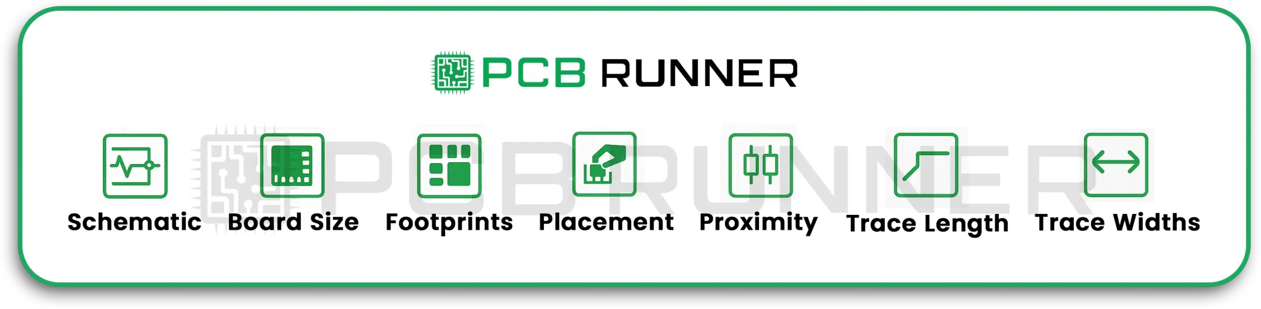
Essential elements of an effective BOM
A well-constructed BOM should contain:
- Name of component and description
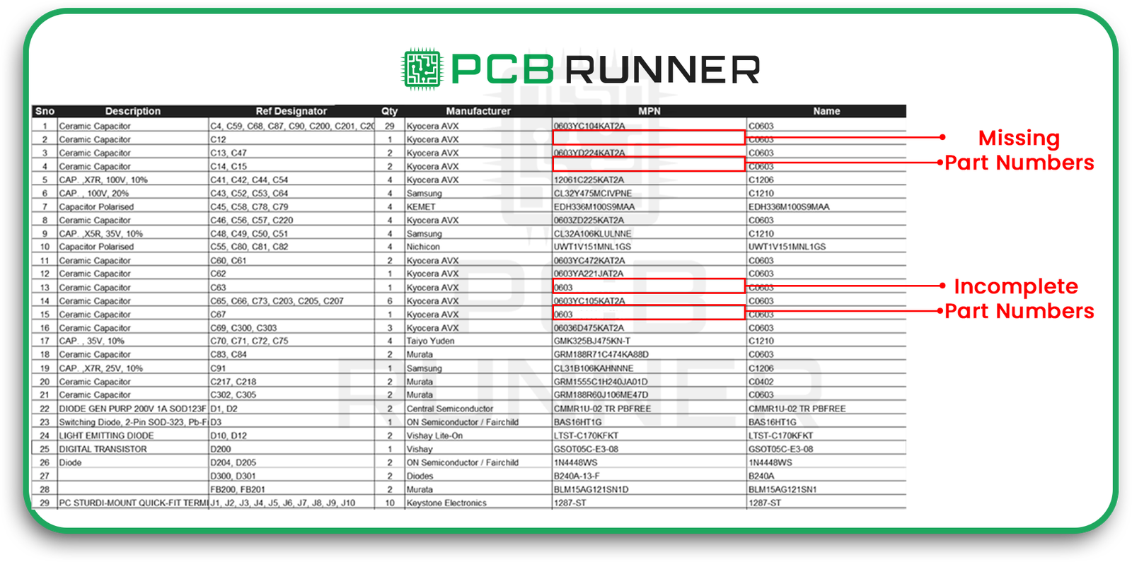
- Part number (PCB manufacturer as well as supplier)
- Units and quantities of measurement
- The footprint of the package and its type
- Lifecycle status (active, obsolete, or NRND, not recommended for new designs)
- Details about the supplier, along with lead times
- Data on compliance like RoHS, REACH
- Version level and revision date
These specifics ensure that every person involved, starting from design engineers all the way to the assembler, works with current, accurate information.
Stakeholders Participated with BOM Management
A BOM isn’t just for designers. It’s a standard document that is used by:
- Designers who develop and keep the BOM up-to-date
- Teams of procurement that source components
- PCB Manufacturers who confirm the availability of parts
- Quality assurance teams that verify product compliance and maintain traceability
In collaborative settings like those of European PCB manufacturing companies, communicating between the various groups is crucial.
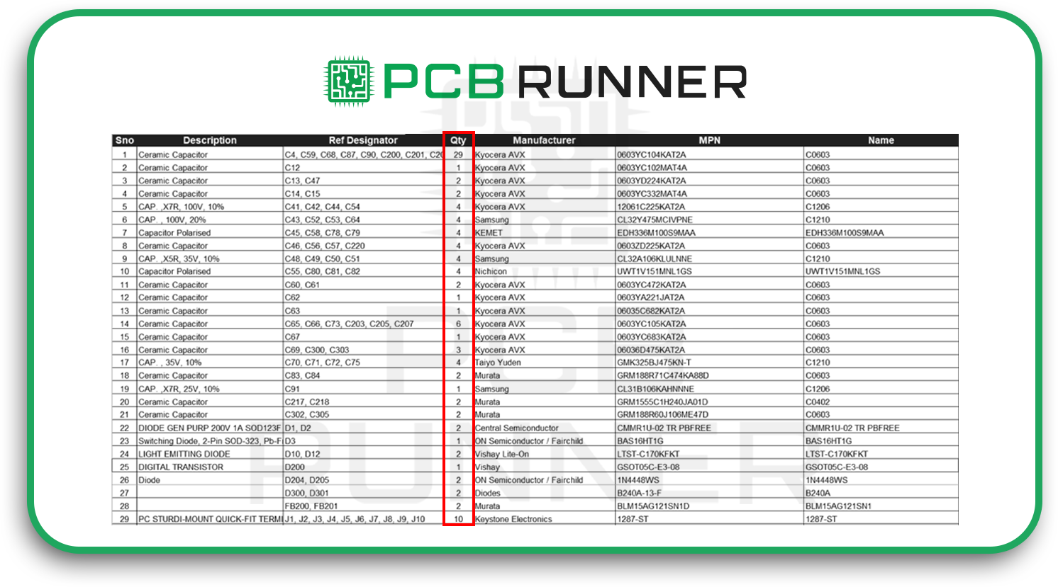
Unreliable Quantities, Units or Measurements
The listing of 10 resistors when the design requires 100 could end the PCB production process. Always double-check the quantities and make sure that all units (e.g. reels, pieces) are accounted for.
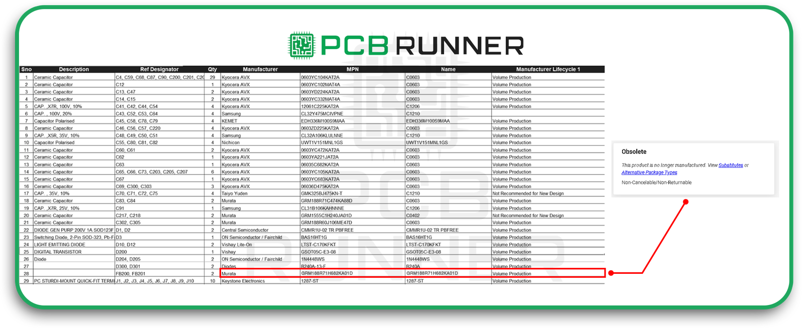
Incomplete Lifecycle Information or Obsolescence Information
Some parts go obsolete quickly. If you don’t have lifecycle information, it’s possible to choose a part that is already removed from production, causing delays until a replacement is discovered.
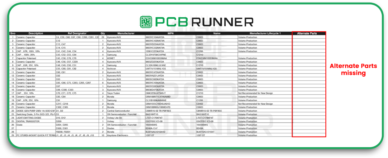
No Substitute or Alternate Parts Listed
In global supply chains, shortages can occur. If you don’t have approved alternatives, your PCB prototype may be delayed for a long time.
Unconcordant Naming and Description Standards
Different styles of naming across teams could confuse suppliers and result in confusion in the order process. A consistent naming style prevents confusion.
Missing Information on Compliance, Regulatory, or Other Data (RoHS, REACH)
European PCB manufacturers are required to comply with RoHS in addition to REACH. The absence of data can end the project during the inspection phase or result in fines for non-compliance.
The absence of a Source or Supplier Traceability
In the absence of a listing of the supplier who originally supplied the component, it can make it difficult to track problems in the future. Be sure to note where each component was purchased.
Duplicate or Redundant Entries
Duplicates can lead to confusion during production, which can increase costs. Regular BOM audits help to prevent this.
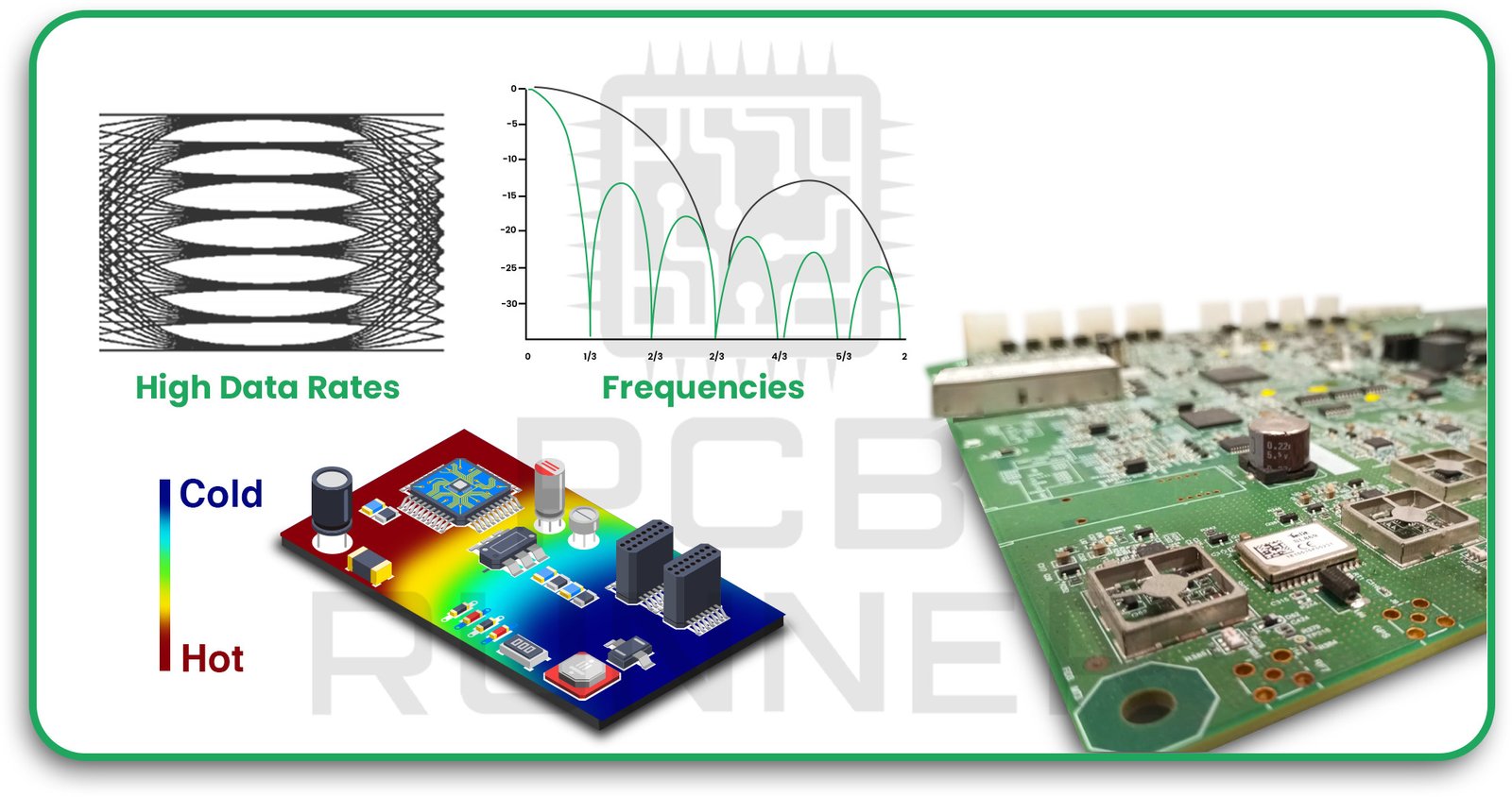
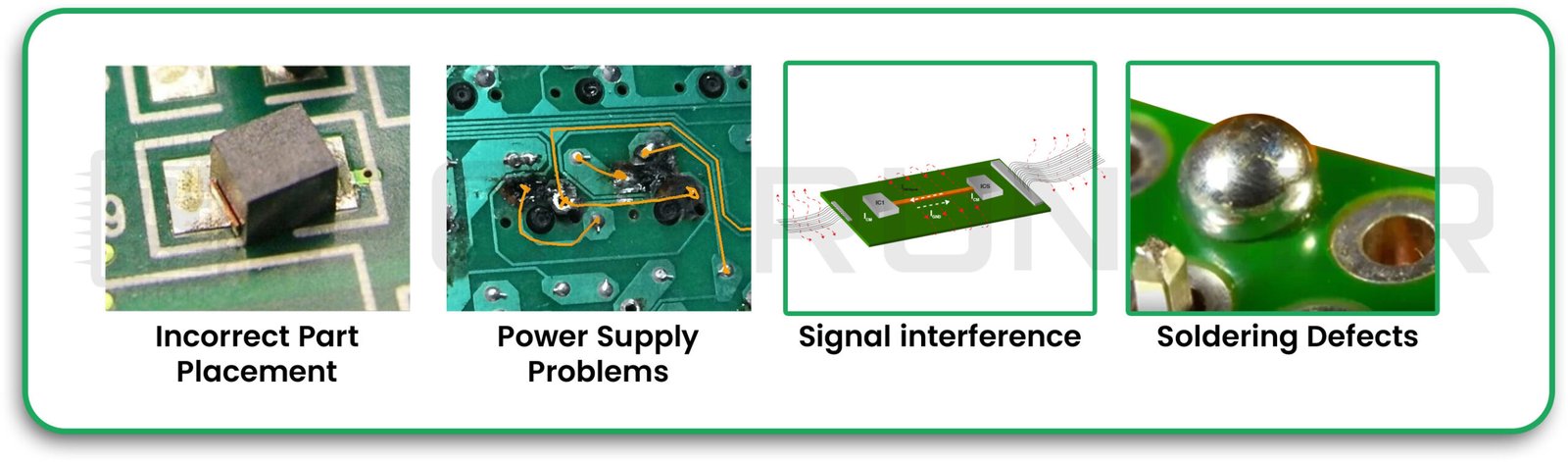
Incorrect Footprints or Mismatched Attributes
If the component footprint doesn’t match the PCB layout, the part won’t fit during assembly. This is one of the most common BOM-related mistakes designers overlook.
BOM Updated Following Design Revisions
When a design evolves or changes, the BOM should be updated accordingly. If not, the manufacturer could produce a different model of the PCB prototype.
Missing Alignment Between Schematic, Layout, as well as BOM
If the three documents don’t get synced, manufacturing errors are virtually inevitable. Automated validation tools can help detect mismatches.
Bad Change Management and Revision Control
Without a clear version control system, teams could use outdated documents or incomplete data. This can lead to confusion and the need to rework.
Insufficient Collaboration across Teams
If the design, procurement and manufacturing teams do not communicate, component selection errors rise. Regular cross-team meetings can prevent this.
How to Avoid these BOM Mistakes: Best Methods
Here’s how you can create a BOM that is efficient in PCB production and production that is error-free.
Commonise Part Numbering and Naming Systems
Create a common part numbering system that is consistent across all teams. This eliminates confusion and enables rapid identification.
Incorporate BOM creation early in Design
Don’t view the BOM as a last-minute addition. Begin to build it along with the design. An early integration can prevent backtracking later.
Conduct Cross-Functional BOM Reviews
Include buyers, engineers, as well as PCB manufacturers in the review. Their inputs together can spot mistakes before they are made.
Monitor Component Lifecycles and Accessibility
Utilise supplier databases as well as PLM tools to monitor whether components are in use, ageing or are out of date. This will prevent disruptions to supply chains within Europe’s market.
Define and Approve Alternate Parts Early
Find substitutes that have the exact requirements. Record these in your BOM to ensure that your prototyping process runs in the event of the time of shortages.
Link the BOM with the Schematic, PCB Layout, and ERP Systems
Integration of these systems guarantees automated updates. The changes in one area will immediately be reflected in all the other areas.
Establish Change Control and Version Tracking Systems
Label each update with the date, version number and the names of the authors. This can help trace the history of design in audits and troubleshooting.
Incorporate Compliance as well as Certification Fields
Incorporate mandatory compliance fields such as RoHS and REACH information. This will ensure European markets are ready and also avoid delays in implementing compliance.
Automated BOM Validation and Consistency Checking
Utilise software to check for missing data, duplicates or parts that aren’t valid. Automated validation reduces time and decreases the need for manual oversight.
Training Teams and Assign Ownership
Every BOM must have a responsible owner accountable for the accuracy of the BOM. Regular training keeps everyone up to date regarding the most effective techniques.
Pre-Submission/Pre-Manufacture BOM Checklist
Before you send your BOM off to a supplier such as PCB Runner, read the following guidelines:
- All Part numbers are verified
- Units and quantities double-checked
- The lifecycle of the product and its availability have been confirmed.
- Alternative parts accepted
- Compliance (RoHS, REACH) confirmed
- Supplier details listed
- The most recent version of the control is used
- Cross-checked with schematics and layout
- File format that is compatible with the PCB manufacturer‘s system
A couple of minutes of verification could make a difference in the amount of time needed for revisions.
PCB Runner offers expert review services to ensure your BOM is accurate, complete, and fully manufacturable. Our expert sales engineers are available at sales@pcbrunner.com.
Conclusion
A clear and well-structured BOM is the foundation of successful PCB manufacturing within Europe. It allows for smooth transitions from design to assembly, decreases the chance of errors, and also saves money and time.
Whether you’re making the prototype PCB or overseeing production at a high volume, making sure you avoid these common mistakes can keep your projects on the right track.
Companies like PCB Runner recognise that precision in the most minor details, for example, a single entry in a BOM, is what ensures accuracy in the final product.
FAQs
1. What exactly is a BOM in PCB manufacturing, and why is it so important?
The BOM (Bill of Materials) lists every component required to build the PCB prototype. It’s crucial because it provides guidance to PCB manufacturers and suppliers throughout the production of PCBs, making sure that all components are in order and readily available.
2. What can I do to avoid mistakes in the selection of components for the design of my PCB prototype?
To prevent the possibility of component selection errors to avoid errors in component selection, always verify the part numbers, verify electrical parameters, and verify footprints. Using certified vendor lists and approved alternative parts can also help reduce sourcing risks.
3. What are the most critical PCB bill of materials tips for newbies?
Top PCB Bill of Materials tips include:
- Begin the BOM at an early stage
- Naming conventions should be uniform.
- Incorporate compliance and lifecycle information.
- Examine the BOM with different teams.
4. What is the lifecycle information that is important in PCB manufacturing in Europe?
In Europe, the environmental standards and availability regulations are stringent. Lifecycle information helps ensure that parts used in PCB manufacturing are compliant, readily available, and not obsolete.
5. Are software tools able to enhance the accuracy of PCB prototype BOMs?
Yes. Many EDA and ERP tools automate validation, detect mismatches, and synchronise design files, ensuring the accuracy and alignment of the BOM with the schematic and layout.