Imagine your TV, computer, or phone. All these devices work thanks to tiny helpers called electronic components. These small parts connect to make a complete electronic system. Without them, nothing would work, not even the lights in your room. But what are these components? Why do we need so many, and how do they work as a team?
Let’s break down the circuit board components that bring every device to life. We’ll use plain language, real-life examples, and clear tips so everyone, even an 8th grader, can understand.
What Are Electronic Components?
Electronic components are the building blocks for every circuit or gadget. Think of them like LEGO pieces for electronics, each has its job, and they all snap together on a custom-printed circuit board.
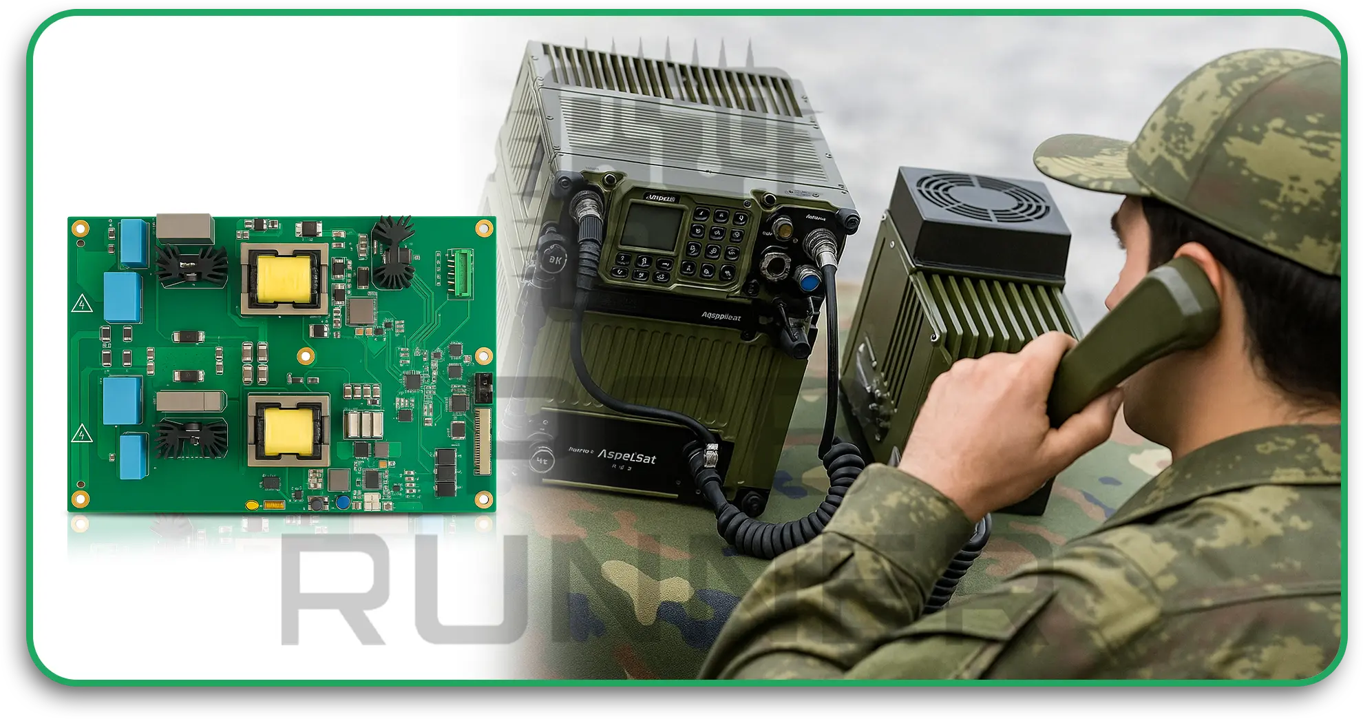
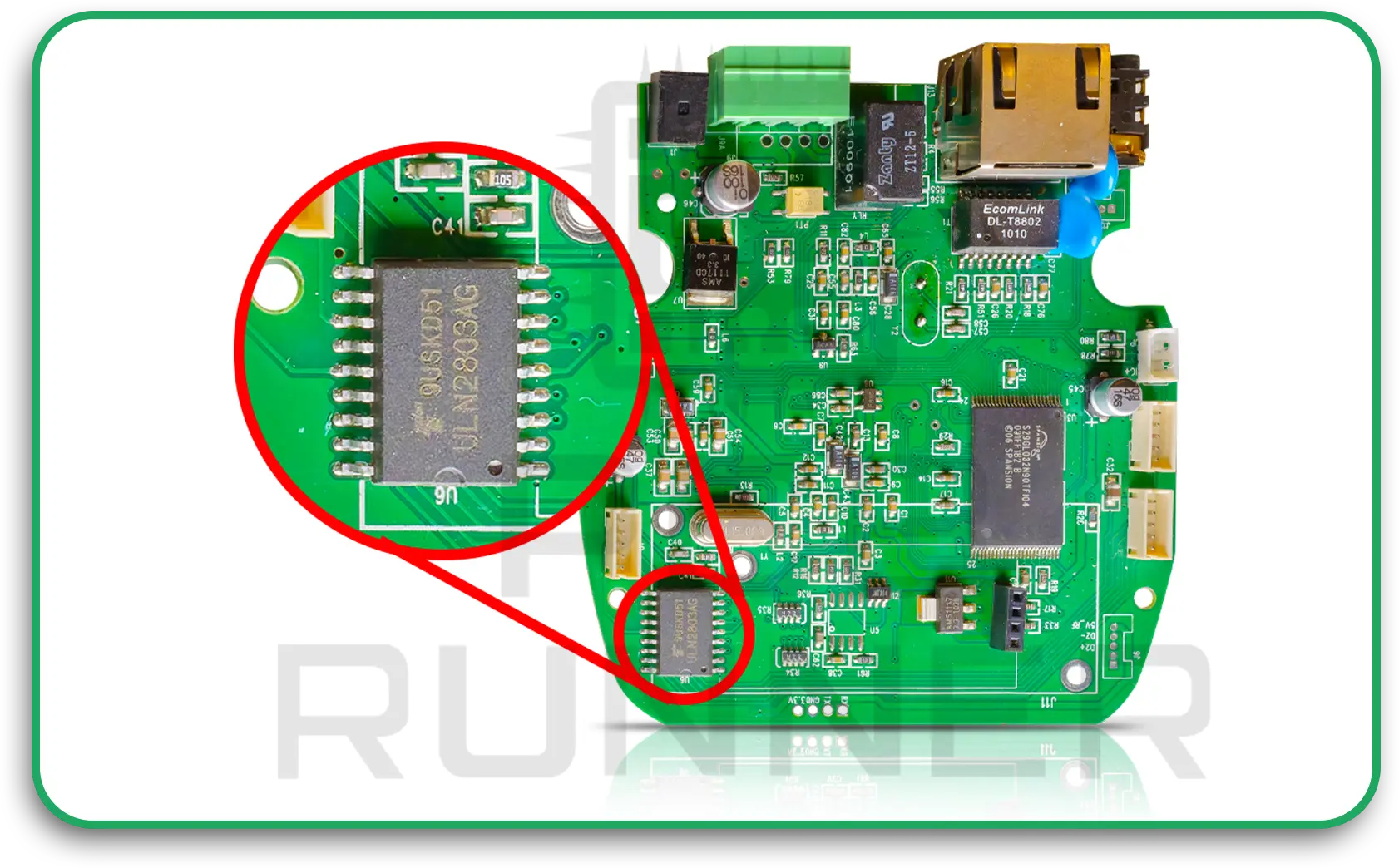
This board, also known as a PCB, holds the parts steady and connects them so that electricity can flow in the correct direction. PCB fabrication assembly is the process of placing these components onto the board, either manually or with specialised machines.
Key Types: Active vs. Passive Components
Electronic parts fall into two main types:
| Type | What They Do | Examples |
| Passive | Cannot create energy, only control electrical flow | Resistors, Capacitors, Inductors |
| Active | Can control electricity and amplify signals | Transistors, Integrated Circuits |
Tip: Most circuits use both types. Passive parts manage the energy, and active ones guide and boost signals.
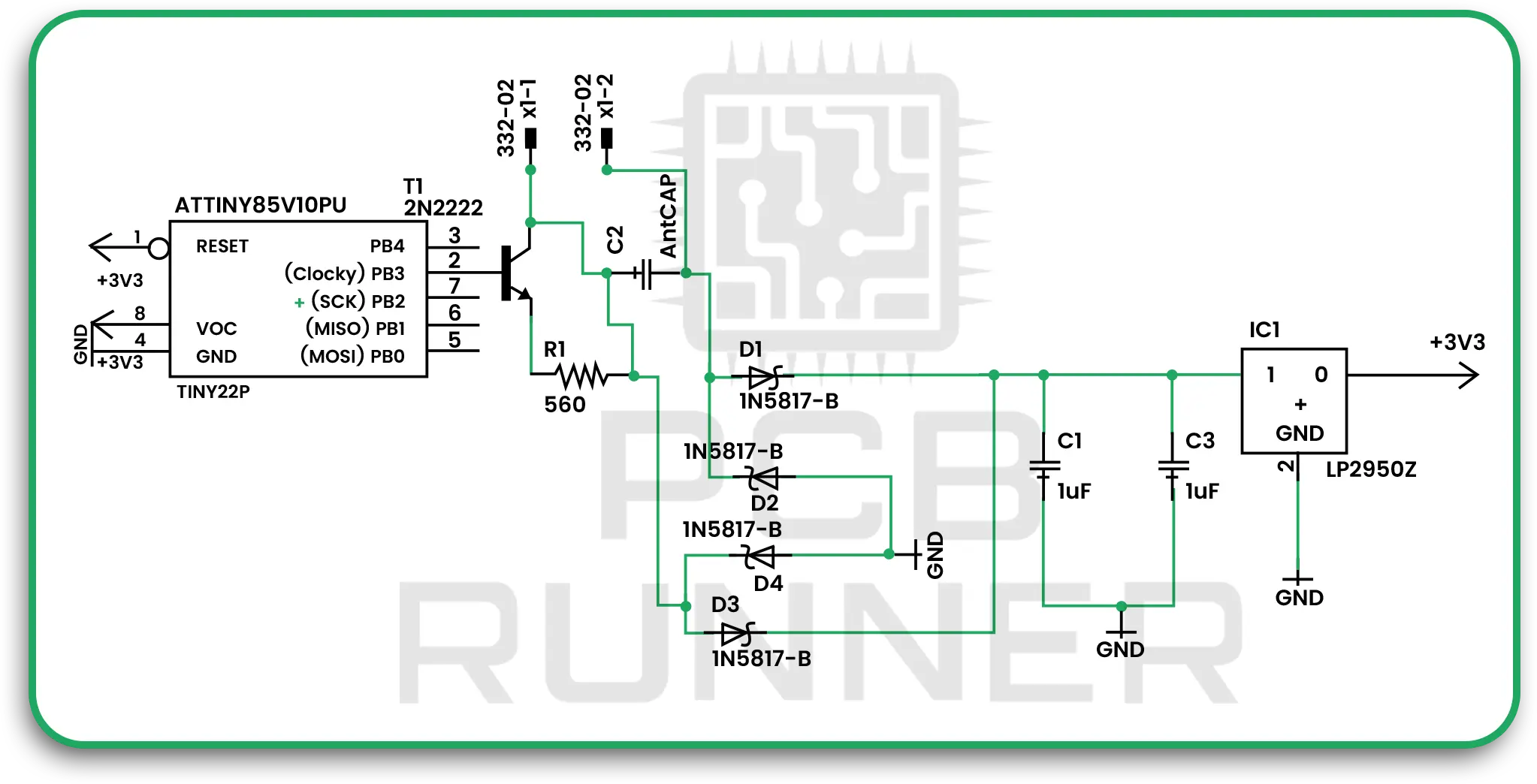
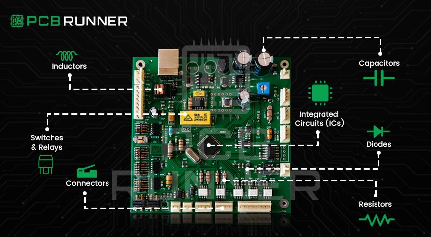
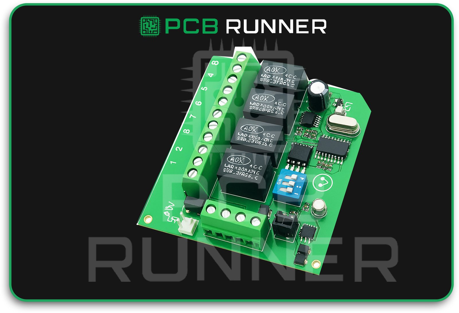
The Main Electronic Components on a PCB
Let’s look at the essential printed circuit board components you’ll find on nearly every electronic device.
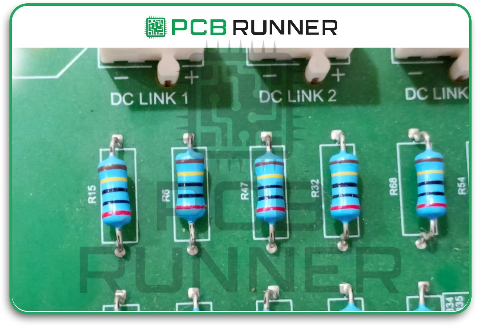
1. Resistors
- Purpose: Slow down or limit the flow of electrical current.
- Analogy: Like squeezing a garden hose to reduce water flow.
- Use: Adjusting signal levels, setting timing, and protecting components from excessive electricity.
If you see colour bands on a tiny resistor, that’s telling you its value.
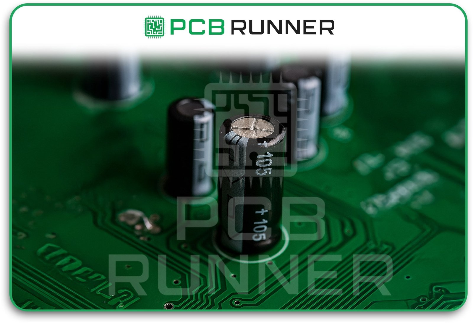
2. Capacitors
- Purpose: Store and quickly release energy when needed.
- Analogy: Like a sponge soaking up water and letting it out fast.
- Use: Smoothing out spikes in electricity, storing power briefly, and filtering signals.
Capacitors come in various shapes and sizes, often resembling small discs or cylinders.
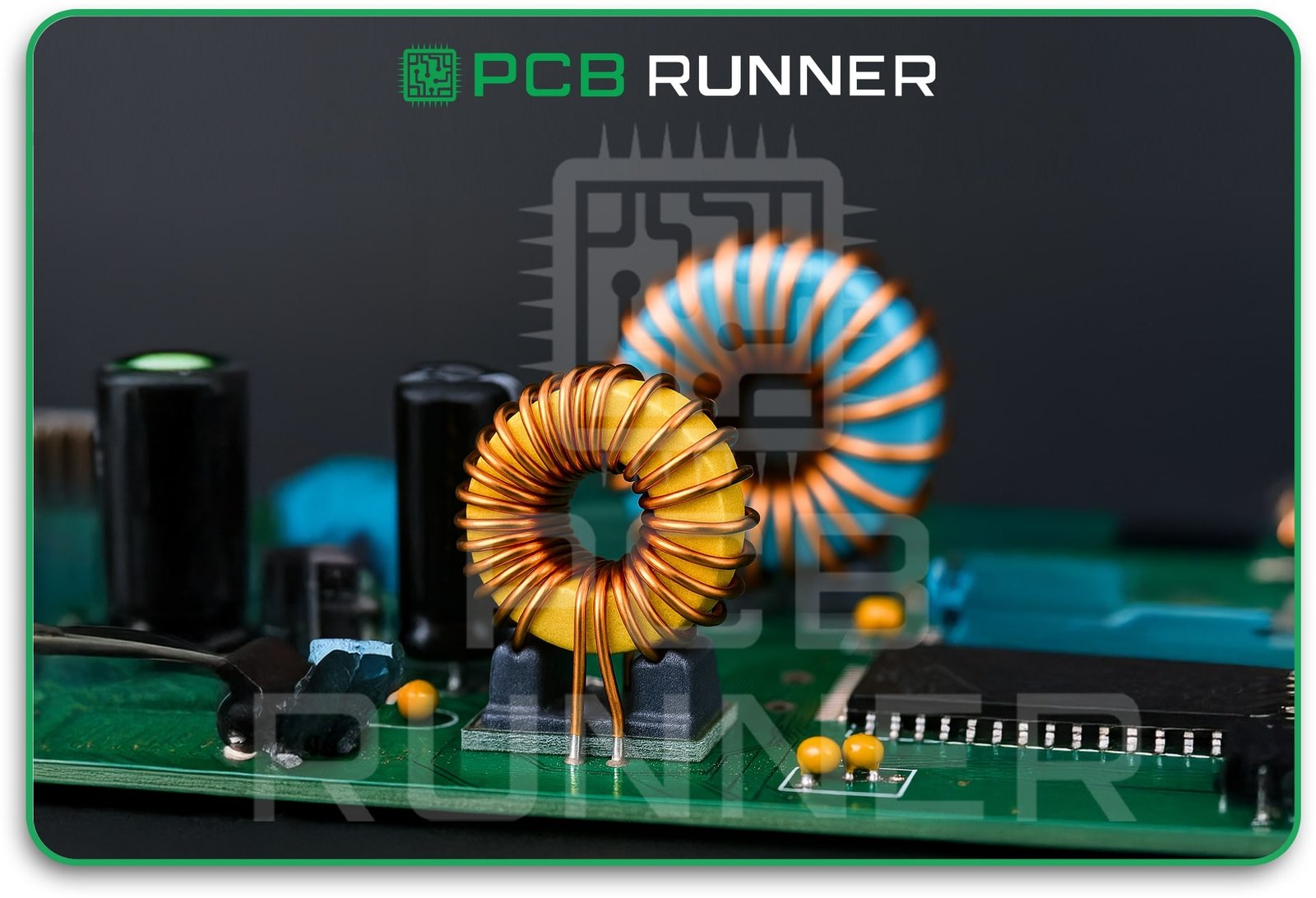
3. Inductors
- Purpose: Store energy as a magnetic field.
- Analogy: Like a coiled spring that stores energy when you press it down.
- Use: Blocking specific signals or helping to create steady power in circuits.
You’ll spot inductors as small coils of wire, sometimes wrapped around a core.
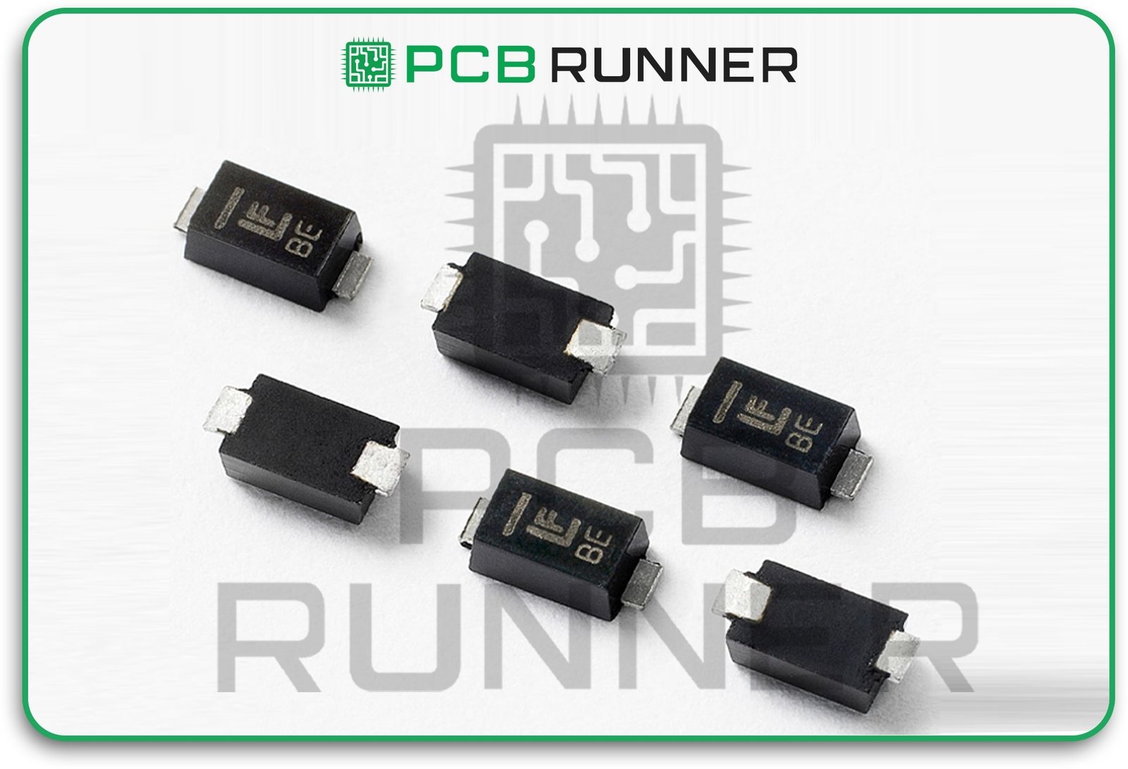
4. Diodes
- Purpose: Let electricity flow in only one direction.
- Analogy: Like a one-way street sign for electric current.
- Use: Protecting other parts from going the wrong way, changing AC to DC.
LEDs (light-emitting diodes) are special diodes that emit light when current flows through them.
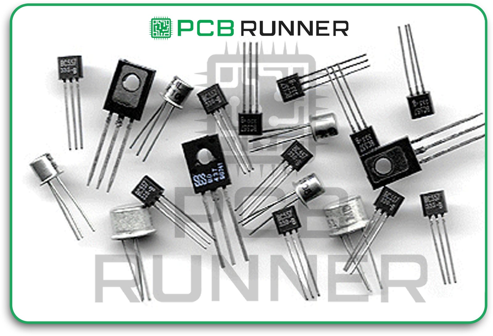
5. Transistors
- Purpose: Act as tiny switches or amplifiers.
- Analogy: Like a gate that can open or close, letting electricity through or blocking it.
- Use: Turning things on and off, boosting weak signals, and acting as brains in computers.
Nearly every modern device has transistors, sometimes millions stacked in a tiny chip!
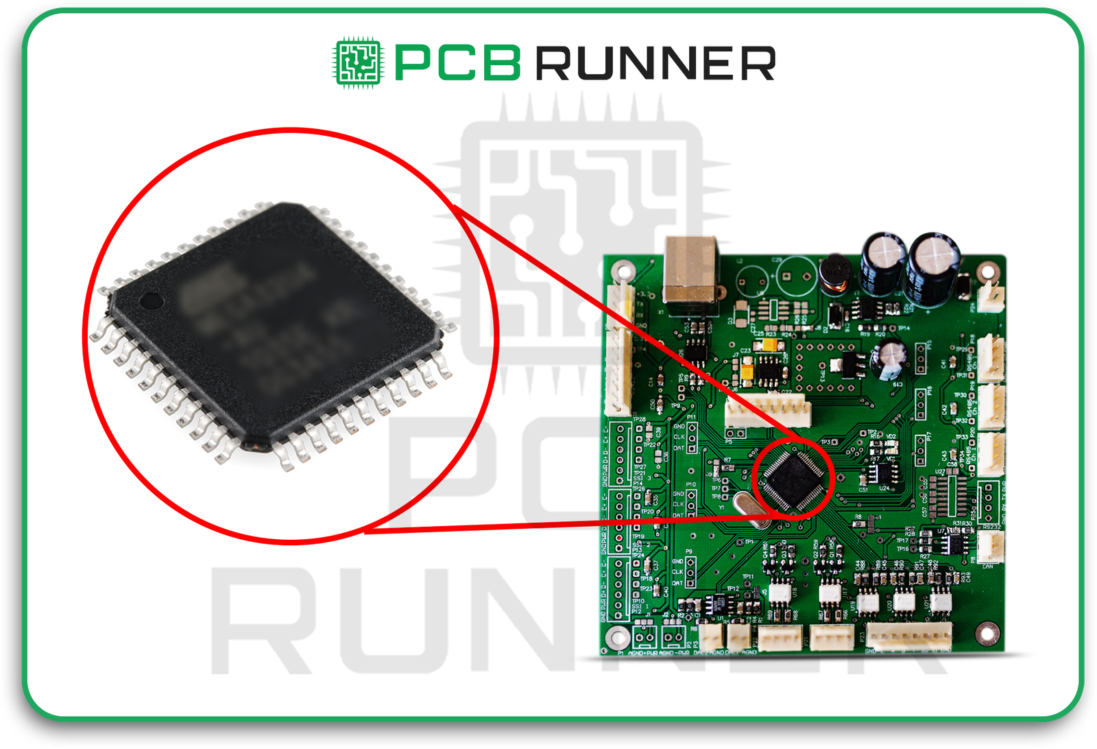
6. Integrated Circuits (ICs)
- Purpose: Combine many components (like transistors, diodes, and resistors) into a single chip.
- Analogy: Like a whole city put onto one piece of land.
- Use: Everything from calculators to computers, radios, and even washing machines.
A single IC can be the brains behind your phone or a simple timer in your oven.
7. Switches and Relays
- Purpose: Open or close circuits by hand (switch) or by another electrical signal (relay).
- Analogy: Like light switches in your house, turn things on or off.
- Use: Control the flow of power, start motors, or change channels.
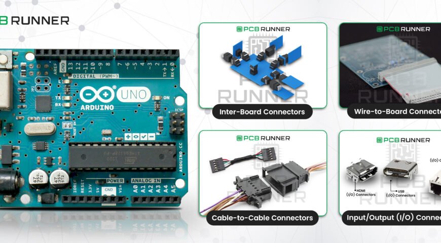
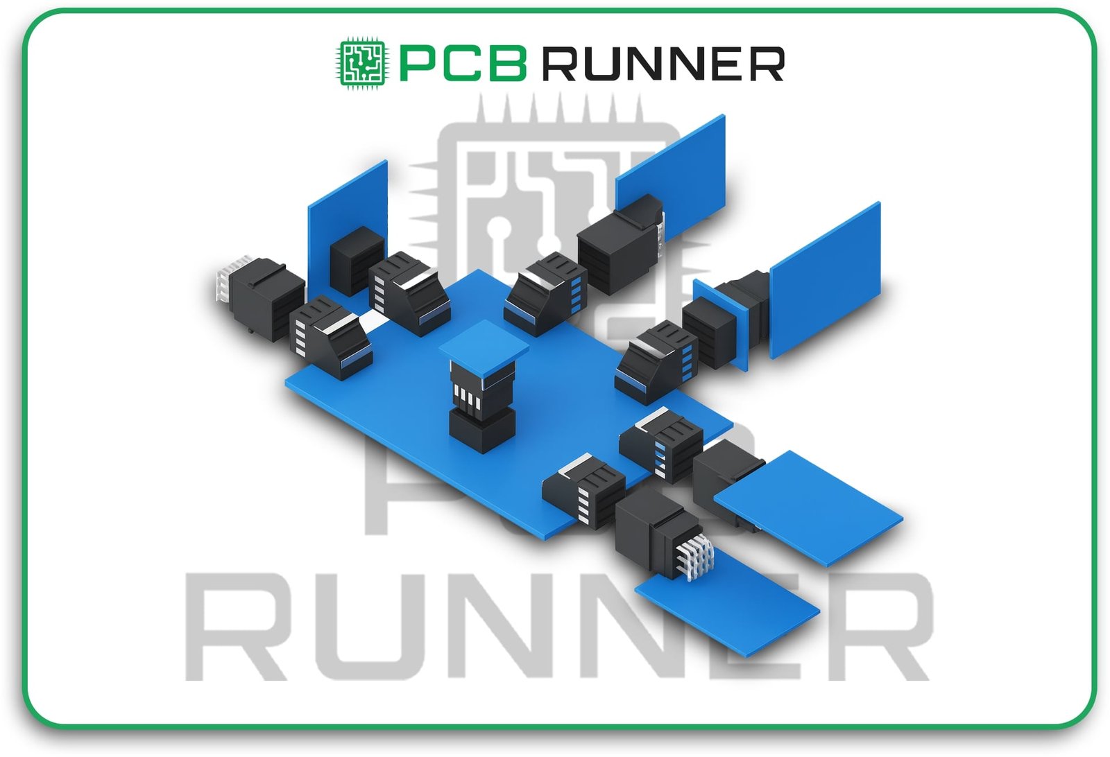
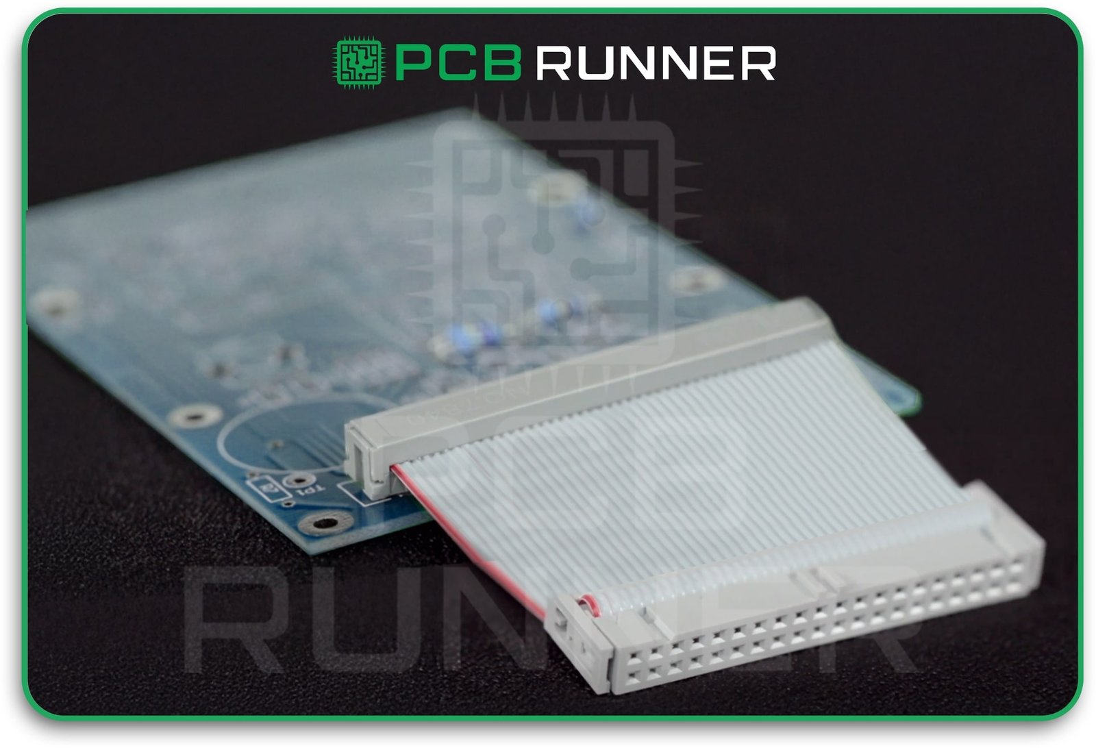
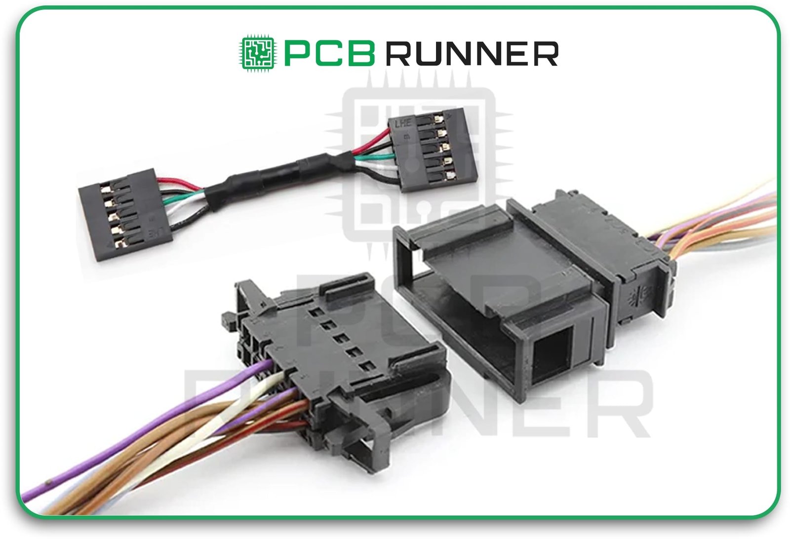
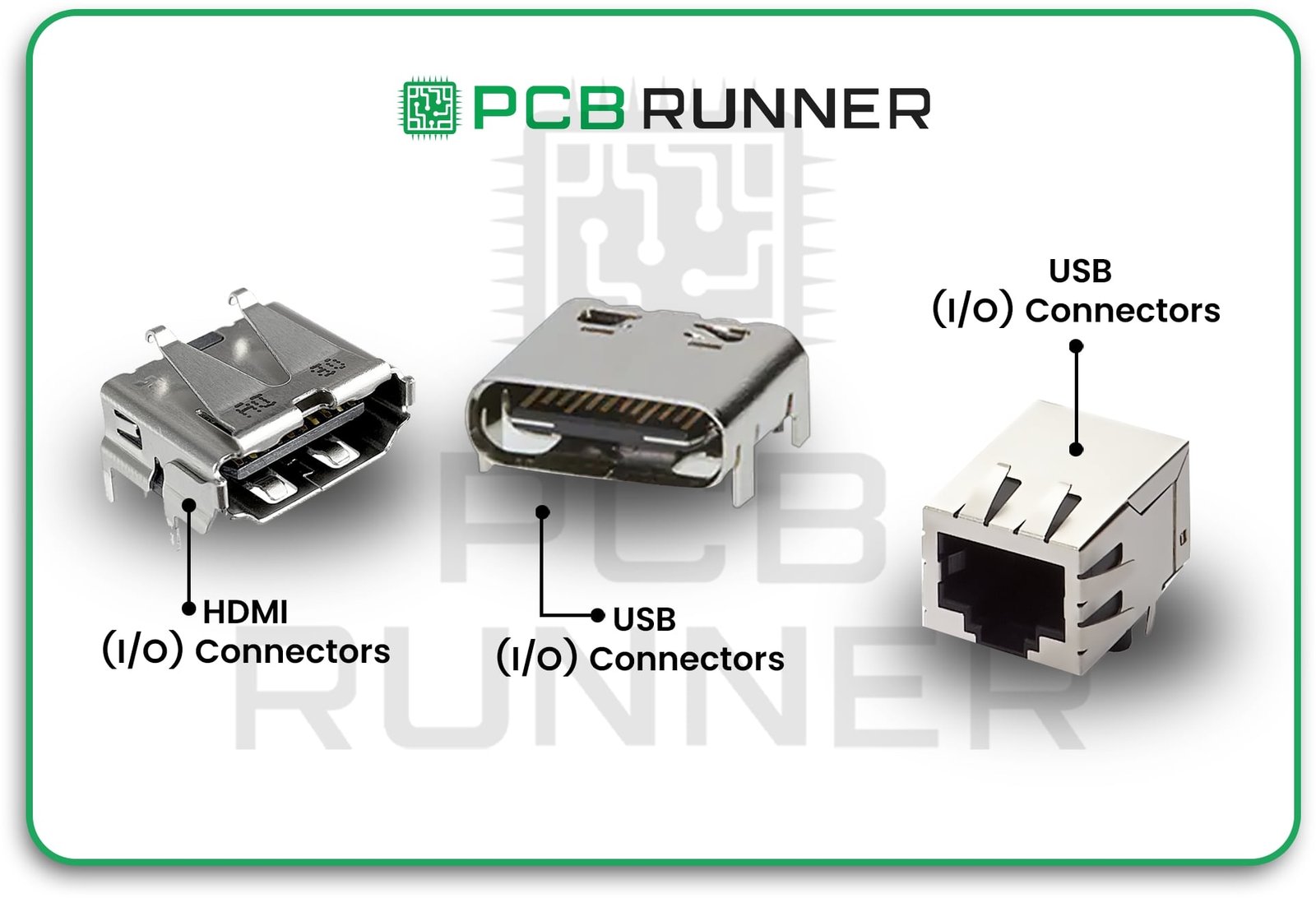
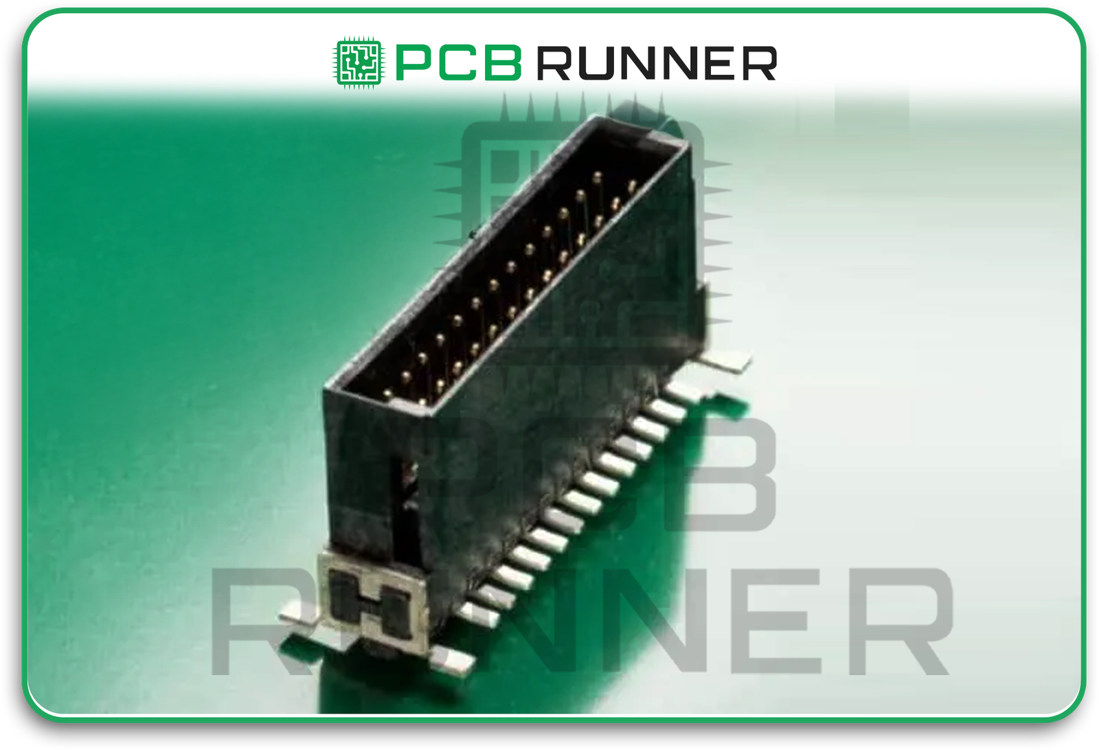
8. Connectors
- Purpose: Join two or more parts of the circuit together.
- Analogy: Like bridges letting cars drive over rivers.
- Use: Connecting batteries, wires, or different boards.
The Role of Printed Circuit Boards
A custom printed circuit board is like a well-designed street map for electricity. The green (or blue) board holds all the circuit board components in place. Thin copper lines connect each pin, directing energy precisely where it is needed. A well-designed electronics board avoids problems like short circuits.
With a complete turnkey assembly, a company handles everything from start to finish. They purchase the parts, assemble the board, solder the components, and test it, ultimately delivering a finished device. For inventors and companies, this saves time and cuts mistakes.
How Do Components Work Together in a Circuit?
Think about a flashlight:
- Battery: Supplies energy.
- Switch: Lets you turn the light on or off.
- Resistor: Limits current to prevent the bulb from burning out.
- LED (diode): Emits light.
If you remove even one part, the circuit doesn’t work correctly. Every component depends on the others.
It’s like making a sandwich, missing bread, meat, or cheese, and your meal isn’t complete.
Common Combinations in Electronics
- Sensor + Amplifier + Display: A thermometer measures heat (sensor), amplifies the signal (amplifier/transistor/IC), and displays the temperature (display/LEDs).
- Radio Circuits: Inductors and capacitors work together to select radio channels.
- Power Supply: Diodes convert AC from the wall to DC for your device; capacitors smooth out the voltage fluctuations.
Collaboration is key! In a printed circuit board assembly, every part has a job.
Tips for Beginners in Electronics Board Design
- Start Simple: Practice with basic kits to see how resistors, capacitors, and LEDs work.
- Use Breadboards: test connections without soldering, allowing you to try new layouts.
- Draw Your Circuit: Map out the placement of each part before building the actual circuit.
- Double-Check Connections: Make sure you haven’t flipped parts or made wrong links, that’s a common mistake!
- Understand Symbols: Learn the standard shapes for each part on a diagram (schematic).
What Is Full Turnkey Assembly?
Full turnkey means “we handle it all.” In electronics, full turnkey assembly includes:
- Collecting every single part (even rare ones)
- Making the board
- Soldering all parts on
- Testing the finished circuit
This is great for inventors, schools, or companies that want to focus on ideas, rather than spending time hunting down pieces.
Real-Life Example: Why Every Part Matters
Imagine building a remote-control car. Inside, your board has:
- Resistors and capacitors to manage power
- Transistors to control the motors
- IC to handle signals from the remote
- Diodes to protect from short circuits
If the car runs too fast and the tires spin out, it’s possible that the resistor wasn’t strong enough. Too slow? The battery may be weak, or a transistor may be failing. Each printed circuit board component affects the overall functioning of the entire system.
Conclusion
Understanding basic electronic components is the first step to making or fixing any electronic device. From resistors and capacitors to transistors and ICs, each part on the custom printed circuit board has a unique role. When you plan a good electronics board design and use professional PCB fabrication assembly or complete turnkey assembly, your projects are more likely to work right the first time.
Every electric circuit is a team effort. Get to know your team, and you can invent, fix, or just enjoy electronics every day.
For advanced help in making, assembling, or testing your custom PCBs, you can turn to fast, friendly experts like PCB Runner, which has supported engineers, students, and industries for over a decade.
Frequently Asked Questions
Q: Why are there so many different kinds of electronic parts?
A: Each part has a special job, like saving energy, blocking unwanted signals, or letting power flow one way. Together, they make devices work as safely and reliably as possible.
Q: Can I use any resistor or capacitor in my circuit?
A: No. Each has a value (such as strength for resistors or storage capacity for capacitors). Selecting the wrong type can cause your circuit to malfunction or even fail.
Q: What’s the best way to learn about circuit board components?
A: Start experimenting! Build small kits, read guides, and watch how each part behaves. Mistakes are a good teacher.
Q: What does “full turnkey assembly” mean for my project?
A: It means experts handle every step, buying, building, and testing, so you get a ready-to-use board without the hassle.
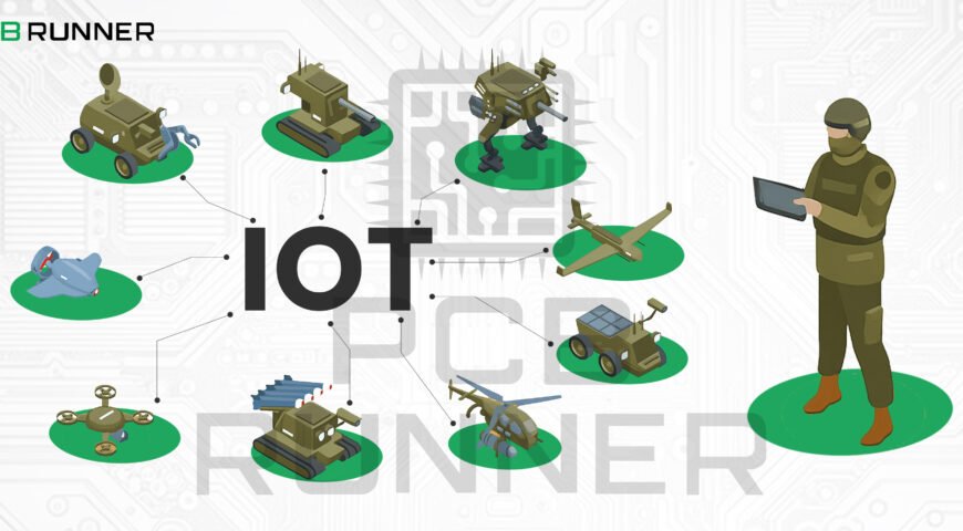
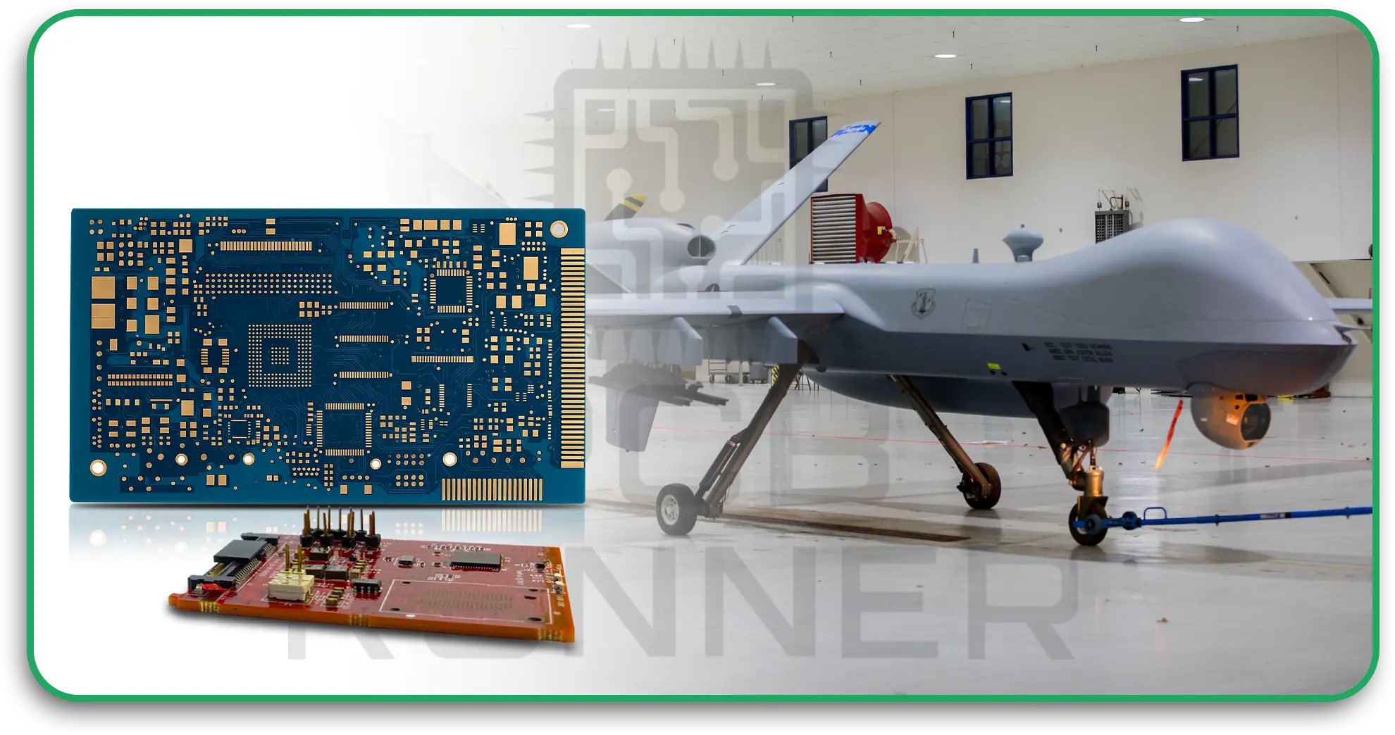
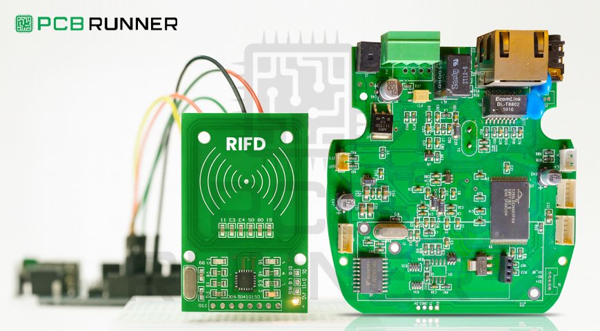
Q: Where are custom printed circuit boards used?
A: Everywhere! Phones, computers, televisions, cars, smartwatches, and more rely on custom-designed PCBs for precise performance.