pcb runner

How the Stretchable PCB Technology Empowers the Future of Electronics

Have you ever wondered how electronic devices are able to bend, twist, or stretch without damage? Electronics are a critical part of our daily lives, including high-tech medical devices and smart fitness trackers. Stretchable PCB technology tackles this issue. Stretchable PCB technology marks a potential shift from traditional rigid printed circuit boards. This technology proves revolutionary as it permits circuits to stretch up to 200% of it’s length like a rubber band.

The goal of this article is to provide a more detailed overview of stretchable PCBs and how it’s using today’s technology to innovate the electronics of tomorrow.

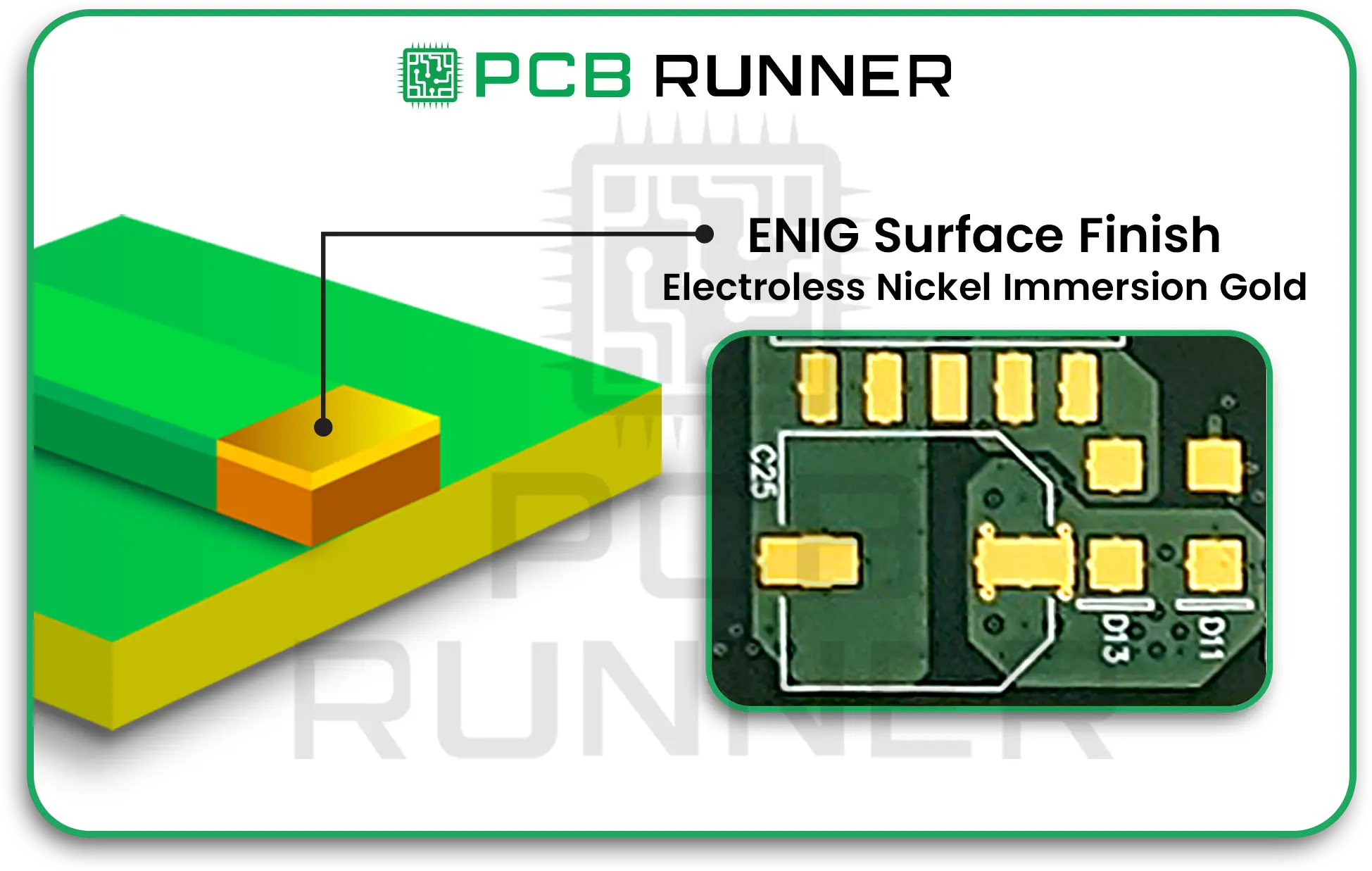
What a Printed Board Stretchable Circuits

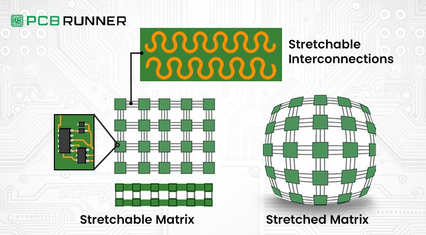
With today’s advanced technology, stretchable printed circuit boards (PCBs) are revolutionising circuitry by using new materials and designs that allow them to bend and twist. Unlike PCBs, which are rigid, stretchable PCBs have the ability to stretch, twist, and bend over 200% of it’s length without malfunctioning.

These PCBs are created using elastic materials along with specific designs, for example, serpentines (wavy lines), which ensure the stretching is distributed evenly across the circuit and no single point is overly stressed and damaged. This characteristic makes them especially helpful in applications where devices have to move or change shape frequently.

Stretchable Circuits

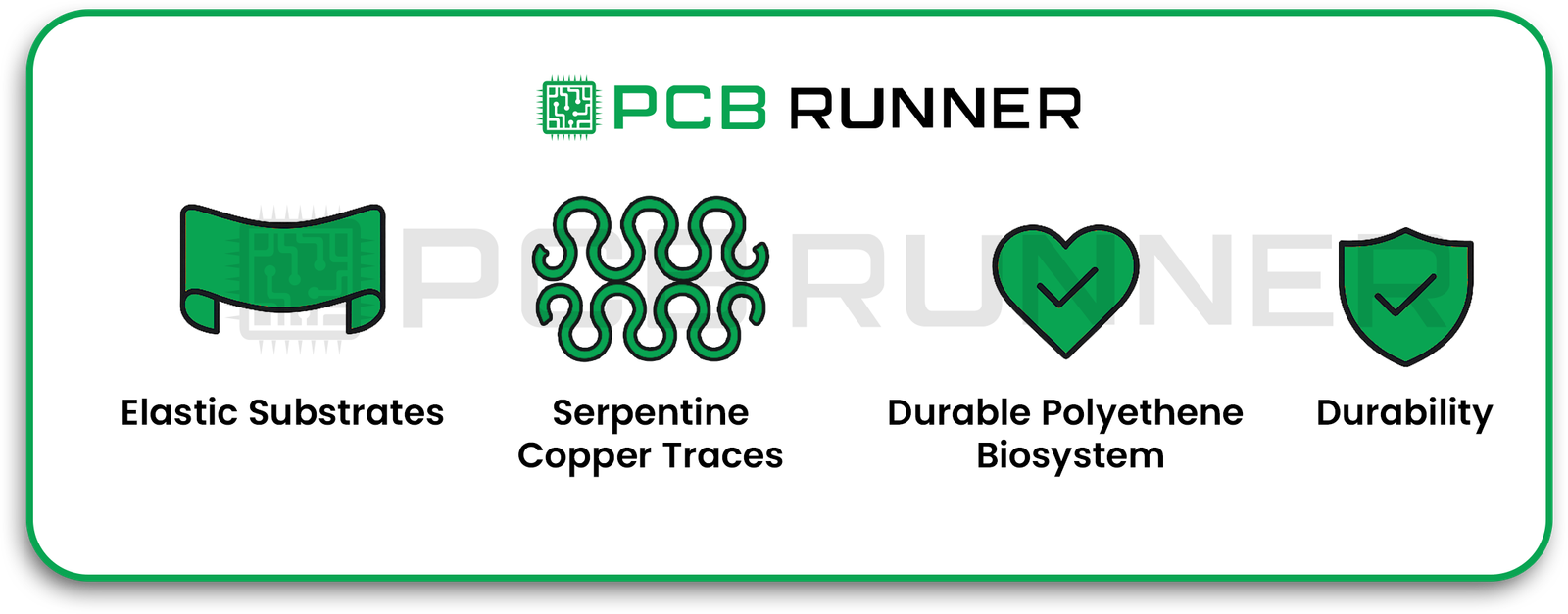
How does the technology for stretchable PCBs work?

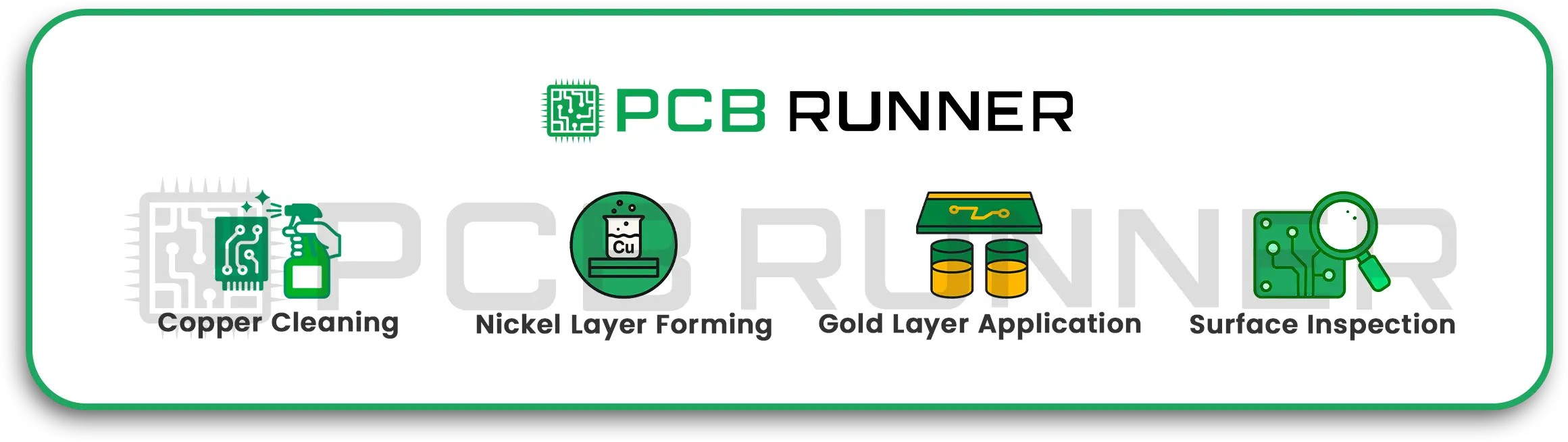
The materials and the designs both have to work in tandem for stretchable PCB technology to function, especially:

  • Elastic Substrates: Rubbery materials such as silicones or specific polymers, which are soft and flexible, are known to stretch and not tear.
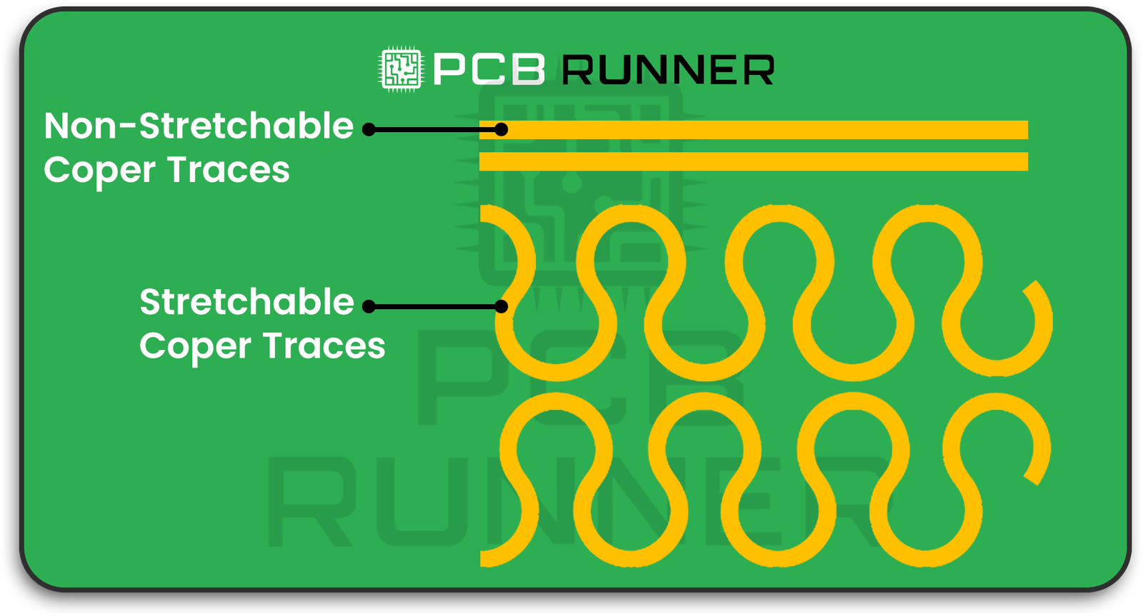
  • Serpentine Copper Traces: The copper lines that transport current are not composed of straight lines; instead, they wiggle in snake-like shapes. Snake-like copper lines are able to stretch and loosen without breaking.
  • Durable polyethene biosystem: This lays emphasis on the rings of the utilised materials, which are safe for the usage of wearing on skin or even fine for surgical implants.

Durability: Thus, PCBs are very reliable in the regard that they may be stretched several thousand times without any loss of function.

stretchable PCBs work

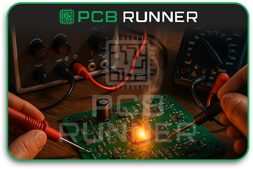
Flex PCB Fabrication and Rigid-Flex Boards

The older stretchable PCBs utilised Flex PCB fabrication or rigid-flex boards. The elderly boards with rigid-flex boards are made from rigid and flexible parts, meant to allow some movement, though overall limited:

  • Flex PCBs are bendable, though they restrict stretching.
  • Combining solid sections that hold maximum stability with flexible sections results in rigid-flex boards that are not stretchable.

Flex PCBs already enable wearables and high-movement electronics. Stretchable flex PCBs take this further by permitting real stretchability, all while ensuring reliability, which deepens possibilities within wearables and other high-movement electronics.  

Where Can Stretchable PCB Technologies Be Applied?  

Stretchable PCBs, Crosswear Ergonomics, and Advanced Materials Creatively:  

  • Wearable Electronics: Smart clothing and health monitors must expand and contract seamlessly. Stretchable PCBs seamlessly support dynamic movements.  
  • Medical Devices: Stretchable PCBs are integral to devices like skin patches, monitoring heart rate, and neural interfaces that wrap around nerves to ensure proper function while allowing user comfort.  
  • Robotics: Soft robots require stretchable PCBs to provide suitable circuits for motion-responsive sensor skins and joints.  
  • Consumer Electronics: Stretchable circuits in new foldable phones and curved screens enable these devices to function even when bent or folded.  
  • Automotive: Stretchable PCBs are essential for sensors in car seats and dashboards that flex with the interior contours.  

All these disciplines gain from the capability to design electronics, not only offering flexibility, but also the ability to stretch and adapt to real-world dynamic shapes.

What Makes Stretchable PCB Technology Essential?

Known electronics can be bulky and rigid, which is a problem for some modern devices. Designers of devices and equipment no longer face rigid boundaries concerning the form of a circuit board with the advent of stretchable printed circuit technology. This signifies:

  • Enhanced Comfort: Wearable gadgets and devices will be more comfortable as they will naturally move along with the body.
  • Improved Durability: Devices will be able to endure repeated bending and stretching without sustaining damage.
  • Advanced Electronics: Devices can be embedded into garments, soft medical implants, or the skins of robots.
  • Enhanced Effectiveness: Even with stretching or twisting, the accuracy of the sensors and components is retained.

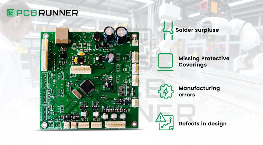
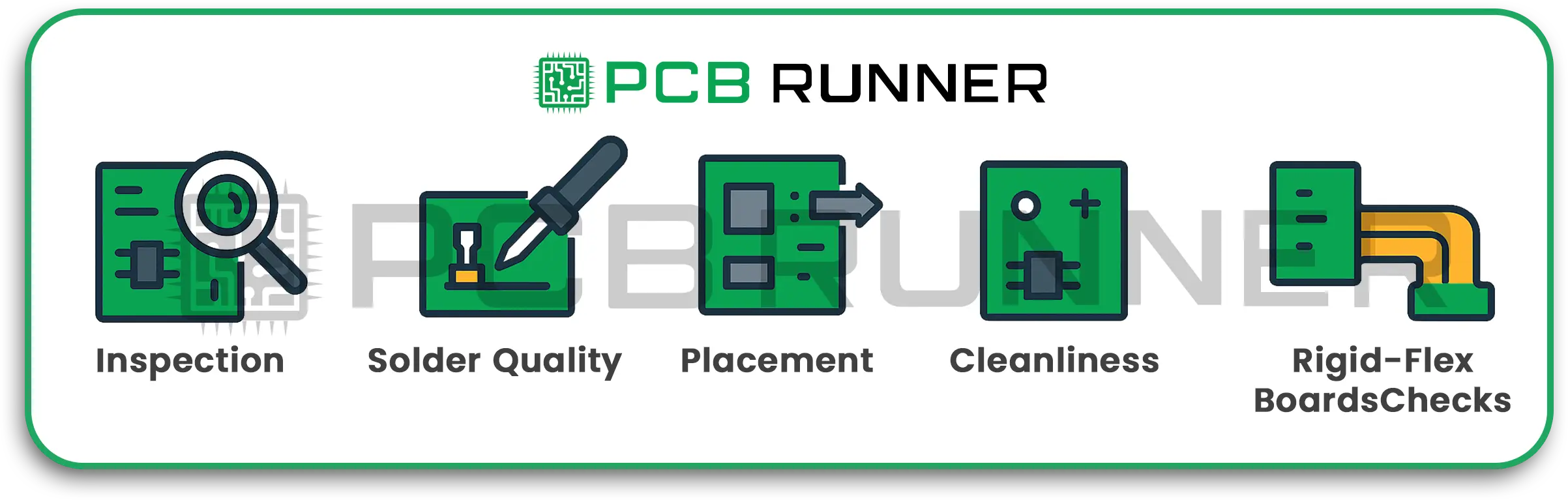
What Are the Issues?

Despite the fantastic capabilities of stretchable PCBs, they do pose a few unique challenges:

  • Specialised materials and careful designs to ensure the circuit’s integrity while stretching make fabrication complex.
  • Regular PCBs tend to be more affordable as compared to these materials and designs.
  • Extreme repetitive stretch or harsh environment testing of the devices is critical.
  • As stretchable PCB technology matures and more manufacturers focus on investment, the unique challenges are bound to lessen.

How to Pick the Optimal PCB Technology  

For designers working on stretchable circuits, these points should be noted:  

  • Know how your device moves: Will it be bending, twisting, or stretching? Only stretchable PCB technology works for devices that absolutely need to stretch.  
  • Analyse the biocompatible option: encapsulation and elastic substrates differ in a wide range for various uses. Consider the medical devices that need such materials.  
  • Work with PCB producers who have vast experience in flexible and stretchable PCB production.  
  • Blend in rigid-flex board designs in portions that require stretchable and flexible elasticity.  
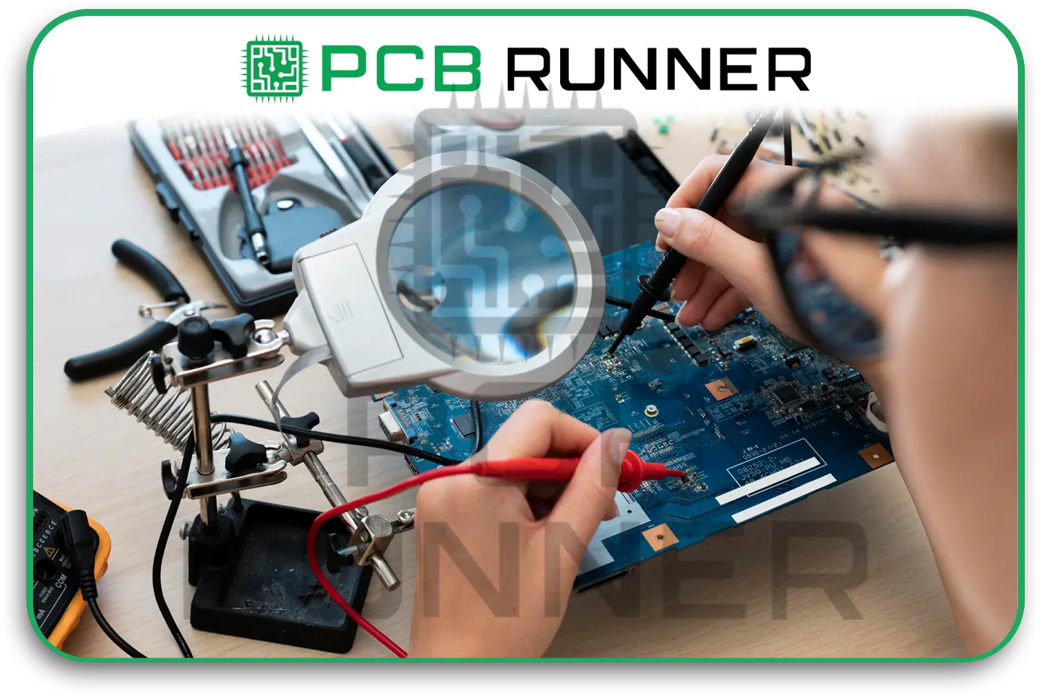
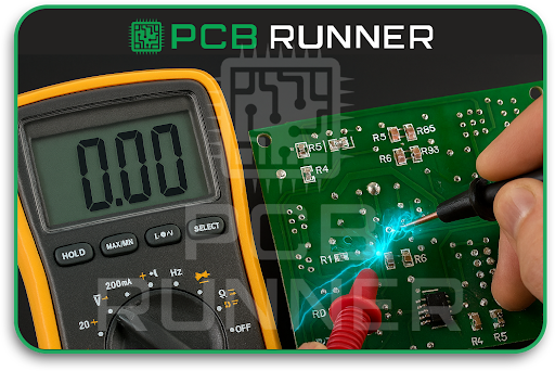
  • Conduct durability and electrical performance tests on the prototypes.  

Stretchable PCBs and the Future of Electronics  

Stretchable PCB technology is making it possible to create extraordinary new devices as electronics shrink and become smarter. Think of medical patches that continuously monitor health stats invisibly, or sensor-laden smart fabrics that change colours in reaction to the wearer’s movements.  

Those boundaries continue to be pushed for stretchable printed circuit boards as researchers find ways to make them stretch even more and for longer. These printed circuits are essential for the Internet of Things, or IoT, as the smart devices need to be well integrated into daily activities.

Conclusion

The stretchable PCB technology serves more than just a purpose; it’s a unique gift of modern engineering that facilitates the flexing of the newest electronic devices. Stretchable circuits improve the functionality of devices in the medical field, robotics, and many other gadgets, making devices smarter and more durable.


Most people are concerned with electronic design and technology innovation, and for them, embracing stretchable PCB technology will be a must for adoption.

At PCB Runner, we help by making these innovations known to designers, engineers, and technology lovers, and in the process, they understand the innovations and stay prepared for the upcoming challenges and innovations.

pcb runner cover

Step-by-Step Guide to Medical PCB Design for Medical Devices

Designing electronics for healthcare is unlike creating boards for consumer gadgets. A single failure can compromise patient safety or lead to costly regulatory delays. This guide walks you through a proven, end-to-end process for medical device PCB design from concept to production by ensuring compliance and reliability.

Whether you’re comparing printed circuit board manufacturers, seeking custom PCB assembly, or planning a full turnkey assembly for high-stakes medical equipment, these steps will help you meet strict quality standards and reduce time to market.
And if you need expert support at any stage, our team is here at sales@pcbrunner.com  to help you move from design to production with confidence.

Let’s start with a question.

If you were designing a medical device, something that a patient’s life might depend on, how much room would you leave for error?

Probably none.

That’s the reality when working with medical device PCB design. These boards go into equipment like heart monitors, defibrillators, MRI scanners, and portable diagnostic tools. In all those cases, failure isn’t just inconvenient. It could be dangerous.

Here’s the thing: designing a PCB for medical devices is not the same as designing one for a smartphone or a smart home gadget. The technical side is more demanding. The regulations are tighter. The margin for error? Almost zero.

So let’s walk through the process step-by-step, from the first sketch to the point where the board is ready to be assembled and tested. I’ll keep it simple, clear, and practical so that you can use this as a real checklist, not just another “how-to” you forget five minutes later.

steps

Step 1: Draw the Schematic

Every board starts with a schematic. Think of it as your map showing how each component connects.

When you’re creating a schematic for PCB assembly for medical purposes, you want to include key details right from the start:

  • The material type you expect to use for the PCB.
  • The power needed for your design.
  • All essential components, placed and connected logically.

Don’t rush this part. Mistakes here will haunt you later in the layout stage, and fixing them later costs time and money.

Schematic

Step 2: Design the PCB Layout

Once you have the schematic, you move to the layout stage. This is where you decide where each component physically sits and how the copper traces connect them.

Most designers use CAD software for this. You’ll import your schematic, then start arranging components in a way that keeps signal paths short and clean.

For medical device PCB assembly, noise and signal clarity are critical. That means:

  • Avoid routing high-speed signals near sensitive analogue lines.
  • Keep critical signals short.

Plan your ground and power planes early to avoid last-minute patch jobs.

PCB-Layout

Step 3: Pay Attention to Critical Medical PCB Factors

This is where many engineers miss details that matter in regulated industries.

Here’s what you should focus on:

  • Component choice: Stick to parts that have proven long-term reliability. Don’t gamble on untested suppliers.
  • Split power planes and proper grounding: Splitting power planes and adding multiple ground layers helps reduce interference.
  • Clear silkscreen markings: Make component labels unambiguous so assembly teams can find precisely what goes where.
  • Signal-to-noise ratios: Medical devices often deal with very low, sensitive signals. Noise on those lines can cause incorrect readings or insufficient data.

If you get just one thing from this section, let it be this: in medical electronics, stability is everything.

Step 4: Review the Bill of Materials (BOM)

The BOM is your recipe for building the board. In medical device PCB design, it’s also part of your compliance record.

What to do here:

  • Confirm every part number and supplier is correct.
  • Read each datasheet, don’t assume a part will work because it looks right.
  • Create an alternate component list in case your first-choice parts are unavailable.

A complete, accurate BOM speeds up full turnkey assembly because there’s no back-and-forth with the manufacturer on missing or mismatched components.

Bom

Step 5: Create an Assembly Drawing

The assembly drawing shows exactly how your finished board should be built.

Think of the assembly drawing as the instruction manual for your custom PCB assembly team. It should include:

  • Component outlines and reference numbers.
  • Polarity markings were required.
  • Notes about special handling or soldering requirements.

A good assembly drawing removes guesswork and ensures that every medical device PCB assembly looks and works the same.

Step 6: Add Test Points

Testing is non-negotiable in medical electronics.

Adding clear, accessible test points during design helps technicians check voltages, signals, and performance without damaging the board. This improves test speed, reduces errors, and makes future troubleshooting easier.

Skipping test points is one of the most common mistakes in PCB design, and one of the costliest to fix later.

Step 7: Work Closely with Your Manufacturer

Here’s what this really means: pick your printed circuit board manufacturers UK partner early, and involve them in the design process.

Why? Because a manufacturer experienced in PCB assembly for medical devices will:

  • Suggest better materials that meet medical compliance.
  • Flag design features that might raise costs or cause delays.
  • Help with documentation for ISO 13485 requirements.

A good medical device PCB isn’t just designed well, it’s also built by people who understand the regulations and demands of healthcare electronics.

Step 8: Meet Regulatory and Quality Documentation Needs

You can’t sell a medical device without paperwork, especially in the UK, EU, or US.

At a minimum, expect to prepare:

  • Design history and change records.
  • Traceability logs for all components.
  • Test records and inspection reports.
  • Verification/validation documentation.

An experienced manufacturer offering a complete turnkey assembly can help generate and store these records for you.

Step 9: Prototype and Test Thoroughly

Never jump into mass production without building prototypes first.

Prototypes let you:

  • Verify your schematic logic.
  • Catch signal integrity issues.
  • Confirm heat dissipation is adequate.
  • Validate assembly instructions and BOM accuracy.

With medical device PCB assembly, multiple prototype rounds aren’t overkill, they’re a smart investment.

Step 10: Move to Production with Full Turnkey Assembly

When the design is solid and testing is complete, it’s time for production.

Choosing a full turnkey assembly streamlines things. It means the manufacturer handles:

  • Board fabrication.
  • Component sourcing.
  • PCB assembly.
  • Testing and inspection.
  • Final packaging.

This approach saves time and keeps the process consistent, which is crucial for PCBs for medical devices.

Step 11: Focus on Long-Term Reliability

Remember, many medical devices run for years without interruption. That means your PCB must be durable enough to handle long service cycles, cleaning cycles, possible heat stress, and occasional mishandling.

Ask your manufacturer about:

  • Conformal coating for moisture protection.
  • High-reliability solder joints.
  • Specialised component mounting for vibration resistance.

Why the Right Partner Matters

Choosing the wrong manufacturer can lead to delays, compliance issues, or even device failures. That’s why partnering with PCB Runner is critical. We specialize in custom PCB assembly for high-stakes industries like medical devices, offering complete turnkey solutions that meet the strictest quality standards. Get in touch with our team today to ensure your medical device PCBs are built with precision, compliance, and reliability from the start.

Working with the wrong manufacturer can cause delays, compliance failures, or worse, device malfunctions. Companies like PCB Runner focus on custom PCB assembly for precisely these high-stakes situations.

They understand the nuances of medical device PCB design, provide complete turnkey assembly, and ensure that every PCB for medical devices meets strict quality standards.

Wrapping It Up

Designing a medical device PCB isn’t just electrical engineering. It’s a careful mix of technical precision, regulatory compliance, and practical assembly planning.

Get the schematic right. Plan your layout to minimise noise. Double-check the BOM. Add test points. Work with a manufacturer who understands the regulatory side as well as the engineering.

Do that, and your medical device PCB assembly will be ready to perform exactly as needed, every time.

And once the boards are built, don’t overlook professional labelling. Partnering with a supplier like Dura Fast Label helps ensure your finished device looks as professional as it performs, with labels that last through use, cleaning, and transport.

If you follow this step-by-step guide, you’ll not only meet the technical and legal requirements for medical PCBs, you’ll also end up with a design you can trust, and so can your end users.

That’s the real goal.

pcb-hardware-debugging

Effective Troubleshooting Techniques for PCB Hardware Debugging

Almost all electronic devices today use a printed circuit board (PCB). Unfortunately, a printed circuit board that is carefully designed and assembled may sometimes malfunction. At this junction, you may have to employ PCB troubleshooting techniques to repair and resolve issues in the shortest time possible. This is especially the case while working on prototypes or bulk orders from trusted assembly manufacturers. Knowing how to debug your PCB is critical in this case.

In this blog, we will highlight the problems associated with PCBs and the solutions that anyone can perform. Methods and tools will be discussed, ranging from basic visual inspections to complex electrical tests. You will learn to diagnose numerous issues and how to isolate problems. Whether you are a beginner or have some experience, these techniques will enable you to resolve circuit board issues more efficiently.

What Is PCB Troubleshooting?

Troubleshooting printed circuit boards, or PCB troubleshooting, is the process of identifying and removing issues that prevent a printed circuit board from functioning accurately. This is often the case after receiving the assembled board, whereby several faults may be present. For instance, the circuit may fail to power on, some components may fail to respond, or some signals may act abnormally.

Every problem requires a definite order of actions to solve it. Start with basic things first before moving on to more complex things. Imagine a detective trying to solve a case; you need to piece together clues to resolve the problem at hand. 

PCB Troubleshooting

Why is it Important to Solve Troubleshooting Issues on PCBs?  

  • Saves time and money: Notice issues early on to avoid expensive redesigns or recalls of the product.  
  • Ensures product quality: The ability to troubleshoot enhances the reliability of electronic products.
  • Speed up prototyping: Working on a PCB prototype comes with a lot of issues that need to be resolved rapidly.  
  • Supports complete turnkey assembly: When you order from circuit board suppliers in the UK & Europe, understanding troubleshooting helps to assure the quality of the order.  
  • Deepen understanding: troubleshooting builds a stronger grasp on how the circuit operates and aids future projects. 

Troubleshooting Issues on PCBs

Common Issues Found on PCB Troubleshooting  

Before attempting to solve issues, it is essential to be aware of the faults you might come across:  

  • Open circuits: Paths that are straight but broken.  
  • Short circuits: Unwanted connections that alter the typical passage of current.  
  • Wrong placement of components: Parts that are installed on the wrong pads or orientation that is flipped.  
  • Cold solder joints: Weak connections due to poor soldering.  
  • Burnt components: Damaged parts that are considered faulty.  
  • Faults in power supply: Voltage drops or instability in power rails.  
  • Integrity issues with signals: Distortion and noise due to poor wiring.  
  • Firmware or software bugs: Issues that are caused due to coding on the board.

At pcbrunner, we minimize these troubleshooting headaches by applying strict manufacturing controls, thorough testing, and design-for-manufacturing reviews so your boards work as intended from the start.

Essential Gadgets Needed for PCB Hardware Debugging

You don’t want to purchase a whole lab setup to get started. Initially, having a few tools is enough and can be expanded upon:  

  • Multimeter: Measures voltage, resistance, and continuity.  
  • Oscilloscope: Used to view waveforms and their shapes.  
  • Magnifying glass or USB microscope: For a magnified view of microscopes and solder joints.  
  • Power supply with current limiting: Used to power a board with a low risk of damage.  
  • Logic analyzer: Used for checking and decoding complex digital signals.  
  • Thermal camera/ IR thermometer: Used to detect components that possibly overheat.  
  • Tweezers and small tools: Tools used to hold small parts that require magnification to be seen.  

Block-by-Block Steps on PCB Troubleshooting Techniques  

1.  Start by looking closely  

Most PCB problems arise from easily overlooked issues. Here are a few of them:  

  • Broken or lifted traces: Looking for marks and scratches on copper with a magnifying glass.  
  • Solder bridges: Pops of solder that are adjacent and blobbed along with solder.  
  • Cold solder joints: Joints that are connected by solder that is dull or cracked.  
  • Foreign debris: Shorts caused by dust and metal that is unwanted.  
  • Overheat burn: Looking for signs of damage or things that are overworked and burned.

Finding and fixing problems visually saves time and effort down the road.  

2. Basic Tasks with a Multimeter  

Your multimeter can also come in handy for simple tasks with electricity:  

  • Continuity test: Make sure the two points that should be connected are connected. A multimeter that beeps indicates a connection. These tests help for open and short circuits.  
  • Resistance measurement: Test suspicious points to see if there is low or high resistance.  
  • Voltage measurement: Carefully power the board and measure key components and essential rails to check for supply voltages.  

Before complex tools are needed, you can focus on problem areas using a multimeter.  

3. Cautiously Observe While Powering Up  

It is essential to carefully power the board as it may be damaged due to existing faults. Follow these suggestions:  

  • Employ a current-limited power supply to help prevent burnouts.  
  • Pay attention to anything unusual that may overheat.  
  • Listen and smell for burning, which indicates shorts and failed components.  
  • Use LEDs or test points to determine if critical areas are powered.  

This step should never be rushed, as sometimes, due to a power issue, several faults tend to be caused that cascade.

4. Focusing on Signal Checking with an Oscilloscope

If functionality appears to be off, check signal waveforms:

  • Are the voltage levels at the expected places?
  • Is the timing correct? (rise and fall times)
  • Is there signal noise or ringing?
  • Use triggers to capture transient mistakes.
  • Using oscilloscopes allows you to validate the logic, confirming that he made the proper validations that were needed while working on the PCB.  

5. Reviewing the Digital Signals with the Logic Analyzer

In cases where the board has I2C or SPI or UART, the board contains I2C or SPI boards, the board necessitates the use of logic analyzers, hence we:  

  • Capture multiple signals and do it at the same time.
  • Decode the communication made.
  • Detect or measure the timing and any data errors.

This is vital and fundamental for the use of microprocessors during the testing of the PCB prototype.  

6. Examine and Restyle the Solder Joints  

In the presence of bad solder joints, there is always the use of:

  • The use of a soldering iron to reflow the joints.
  • Use of a solder wick to get rid of bridges.
  • And, the use of flux enables the solder process to flow better.  
  • Good joints remain vital in the electronics domain and correct undead devices as per the working.

7. Software and Firmware Examination  

In the presence of PCBs having programmable devices:  

  • Confirm if the firmware has been flashed the right way.
  • Confirm the correct way with debugging tools while processing the code.
  • Confirm the running of the software with good hardware to know the defects.  

In some cases, it is the software that causes the entire facade of the hardware failures.

Tips for PCB Troubleshooting Success

  • Document everything: Capture notes and take photos during the debugging for future reference.
  • Divide and conquer: Take problems on the board in sections so as to lessen the workload.
  • Stay organized: Maintain a neat work area that is well-lit, has all the required tools.

Contact our sales engineer at sales@pcbrunner.com to discuss design goals, get a production estimate or explore how our pcb prototype expertise can streamline your next build.

Conclusion

Troubleshooting a PCB does not have to be a stressful experience. Follow the steps of inspection, measurement, powering the device, and analyzing signals, and you will be able to fix most of the hardware issues.

Here at PCB Runner, we maintain a high standard of quality from prototyping to full production. However, knowing the PCB troubleshooting tips provided will help you get the most out of your boards, no matter what stage you are at.

Embedding Components in Printed Circuit Boards

Key Techniques for Embedding Components in Printed Circuit Boards

Designing  custom printed circuit boards for today’s compact, high-speed electronics requires more than just traditional surface mountain. Engineers face shrinking form factors, heat management challenges, and signal-integrity issues. Embedding components inside the board itself addresses these constraints.

The printed circuit boards are the brains of any modern device. When designing or fabricating a custom printed circuit board, integrating components into the board can be more efficient with regard to area, performance, and reliability.

This blog outlines the techniques of embedding components into PCBs. 

Embedding Components

Methods of Integrating embedded components into printed circuit boards

Printed circuit boards traditionally mount parts on the surface. But embedding changes the game. In a custom printed circuit board or DI printed circuit board, passive parts and even ICs can be laminated inside the stack.

Embedding:

  • Enhances the complexity of the design and the density of the layout without enlarging the board.
  • Shields components from mechanical wear, dust, and damage.
  • Shortens signal pats, improving accuracy and speed.
  • Enables the development of lighter, smaller, and more reliable devices.

The trend of miniaturization is more noticeable with advanced printed circuit boards, like HDI printed circuit boards or specialized ones.

Embedding

Benefits of Embedding Components

The advantages of embedding components on a circuit board are the following:  

  • Space Saving: Embedding either increases the surface area within the circuit board for the addition of other parts or reduces the surface area of the PCB overall. This is crucial for wearable electronics.
  • Enhanced electrical performance: Internal component placement reduces parasitic effects as well as signal interference when compared to external component mounting. This increases accuracy and speed.  
  • Greater reliability: Parts that are embedded are more reliable when it comes to protecting against mechanical shocks, dust, or corrosion.  
  • Reduced soldering steps: Embedding cuts the number of solder joints and placements, lowering assembly errors and shortening production time.  
  • Some embedded approaches enhance the dissipation of heat, which improves thermal management.  

At pcbrunner, we specialize in PCB embedding solutions that bring all these advantages into your design.

Key Approaches to Embedding Components in PCBs

There are other approaches to the embedding of components in printed circuit boards, other than the component placement:  

Creating Cavities or Slots in PCB Layers

This approach is cavity embedding:  

The precision cavity approach involves the machining or laser drilling of the recesses into the PCB layer. This technique is often referred to as cavity embedding.  

Chips or components are placed into the recesses so that they are flush or below the layer surface.  

The parts are secured to the recesses using adhesives.  

Subsequent layers of prepreg or a core layer are added to the initial layers to seal and build the stacked PCB.  

This technique is mainly applied in the embedding of passive components such as resistors and capacitors, as well as thin IC packages. They enable better integration without the addition of surface board thickness.

2. Sandwiching Parts Between Prepreg Layers

Prepreg materials are crucial in PCB lamination. Manufacturers:  

* Position components between sheets of prepreg (semi-cured resin sheets).

* Stack several prepreg and core layers containing parts within them.  

* Heat and apply pressure to cure the stack to create a single, solid, bonded piece.  

This method effectively incorporates both active and passive components. It is essential to control material thickness to avoid warping the board.  

3. Via Connections and Laser Drilling

The rest of the board requires electrically connecting the embedded parts. Laser micro-drilled vias do the following:  

* Drilled access holes to reach pads on the embedded components.

* Currently used to conduct the vias with copper electrically.  

* Attach embedded components directly and eliminate the need for long traces.  

This is especially important in HDI printed circuit boards for the backbone of connecting hidden components in restricted spaces using laser via technology.  

4. Embedding with Film

Thin substrate materials are transformed into flexible ones using:  

* Thin polymer films are used to place components on.

* Films are then incorporated into multilayer PCBs.  

This is important for flexible and bendable PCBs where there are no rigid cavities.

5. Additive and 3D Printing Techniques (Emerging)

A few manufacturers are looking into 3D printing and additive manufacturing for embedding:

The addition and layering of particular conductive and insulating materials.

There are mid-process component integrations.

While they are still in the experimental phase, this could enable incorporating more intricate designs with different geometries.

Prototyping Considerations for PCB Prototypes with Embedded Components

Before moving to mass production, it’s a smart idea to build at least one PCB prototype with the planned embedded components. Working closely with your PCB supplier early on helps you to understand key process limits like how deep cavities can go, the tolerances for laser-drilled vias, and the thickness of prepreg materials. By adjusting your design to fit within these limits, you can avoid expensive rework later and get your product to market faster.If you’d like expert support with prototyping or need clarity on design tolerances, our team is here to guide you through every step before mass production to contact our sales engineer contact us today at sales@pcbrunner.com

Tips for Designing with Embedded Components –

Get the order right for cavity and embedded components placement: The PCB thickness and spacings between layers to be mounted must be considered.  

  • Don’t overly restrict space for routing: Space for routing and connections must be available for laser-drilled fine vias.
  • Consult with the suppliers: Component embedding feasibility can be confirmed with suppliers.
  • Respect weak zone distances: Minimum distances around embedded components are short, weak zones, or damaging structural integrity.

What are the Impacts of Embedding on the PCB Fabrication and Assembly Processes? 

The addition of components that embed firmly changes the entire PCB production life cycle:

  • Fabrication complexity: undergoes changes with layering precision, requires specialized equipment (laser drills), and careful pre-cured board stacking for uniform board thickness.
  • Blind and active inspection: embedded components require specialized X-ray inspection methods for verification of placement and connection for the part hidden in the layers.
  • Assembly: the surface-mount assembly stage is less. But requires high-level precision in PCB layout to ensure that all embedded components interface appropriately with via nets. Embedded components must withstand the temperature and pressure of lamination.
  • Cost: Embedding parts increases the cost. But, in most cases, production cost and time are reduced, and the entire system size and intricacy are increased.

HDI Printed Circuit Boards and Embedding 

Mobile and aerospace industries utilize HDI (High Density Interconnection) PCBs. They are embedding-enhanced for increased efficiency:

  • Incorporating passive components into HDI stackups helps to reduce the number of board layers.
  • Permits the use of small microvias and laser-etched cavities to densely pack functions.
  • Increases signal integrity and improves reliability for high-speed designs.

Conclusion

Integrating components into printed circuit boards eliminates several steps in the processes of miniaturizing and accelerating the efficiency of electronic devices. Manufacturers are able to make custom printed circuit boards and HDI printed circuit boards using advanced techniques like cavity creation, prepreg lamination, and laser via truly remarkable connections.  

Whether you are designing a PCB prototype or strategizing for large-scale production to know how embedding techniques interact with circuit board components. For further guidance, reach out to PCB Runner.  

PCB innovations

The Future of Electronics: Innovations of Global Importance

Smartphones, laptops, TVs and smart watches, nearly every room today is filled with electronics. It is wondrous to think, what is next? Innovations in design, new materials, and technology shifts are moving the electronics world at full speed. In this blog, we are going to explore the key trends, remarkable innovations, and essential factors regarding the future of electronics. Also, we will encapsulate how innovative technology is leading us to a greener future, along with the advanced manufacturing processes of tiny circuit boards.  

The electronics industry is growing at an astonishing pace. It is anticipated to be worth hundreds of billions of dollars with an ever-increasing smart device and aid bazaar. From grocery lists to talking with your refrigerator, we already have smart devices with almost limitless capabilities. The future holds cars that drive themselves and early illness-detecting tiny devices for medical applications.  

As the industry shifts, designers, users and those that rely on these devices are in for a remarkable surprise. Let us explore what is on the horizon and what that means for the common folk. From extraordinary healthcare devices that are implants to robotics and AI-integrated vehicles, the future of electronics remains limitless.

The PCB: Understanding Electronics as a System

At the heart of all modern electronic devices, such as smartphones and car dashboards, printed circuit boards (PCBs) serve a critical role as the “nervous system” of any device. Just as the nervous system integrates and orchestrates activity throughout an organism, PCBs connect and integrate all the device components. For the more complex devices like medical devices, PCBs play an equally critical role in performing and ensuring the device functions accurately and effectively.

Understanding Electronics as a System

Why PCB Technology is Imperative to Electronics

  • Reliability: All electronic devices, such as smartphones, must serve their intended purpose at all times.
  • Advanced miniaturisation: As modern electronics shrink, PCBs are required to integrate components into a shrink in footprint.
  • Custom Designs: As the diversity in the population changes, the device functionalities must serve the needs of the modern-day individual.
  • Sustainability: Business and manufacturing of electronics are shifting towards employing fewer materials and zero-waste manufacturing.

PCB Technology

Innovative Trends in PCB Manufacturing

Innovation trends in PCBs are meant to capture the interest of electronic enthusiasts. To capture the interest of electronic enthusiasts, the leading manufacturers of PCB circuit boards are going beyond ‘green boards’ by using unique materials and advanced modelled structures to create broader and more complex functions.

1. 3D Printing and Prototyping

Picture this: you can now print a customised circuit board nearly as effortlessly as printing a photo. 3D printing boosts productivity and improves the rate at which concepts are turned into products while reducing waste.  

This accelerates the journey from inspiration to implementation and accelerates market availability.  

2. Smarter Automation and Robotics  

Faster output and quicker inspection of tiny chips and boards is now possible with robotics.  

This translates to improved accuracy, less rework, and quicker availability in the market.  

3. Rigid Flex and Rigid PCBs: Flexible, Yet Strong  

These are used to manufacture thin and lightweight gadgets, including wrist watches and hearing aids. Smartwatches are also designed using this technology.  

The reason why fitness trackers and phones are slimmer and can even bend is due to rigid flex PCB technology. This technology combines rigid sections that provide toughness with flexible sections that are able to assume different and intricate shapes.

Electronics PCB Assembly: Improving Efficiently Each Day

After assembling and preparing the board, the next step is to incorporate its components: the connectors, sensors, and chips. Here is the update that the PCB fabrication assembly is receiving:

  • Surface Mount Technology (SMT): Specifically for miniaturised chips, it is encapsulated and placed on the surface, allowing your devices to perform more advanced feats while maintaining a small and compact silhouette.
  • Advanced Materials: Graphene and ceramics are shifting the gadgets industry and allowing the products to have a longer life span. A device, even when used nonstop, will continue to run cooler.

Smart cameras and sensors are able to perform more complex and advanced inspections. Devices with such automated inspections have higher quality standards.

Global Trends: What’s Powering the Future?

There is more to the devices than “smaller and portable”. These macro changes are the foundation for the outlook of electronics:

1. The AI and IoT Revolution

Smart devices are becoming more commonplace, and the forecast for IoT devices is beyond 25 billion.

Artificial Intelligence is ubiquitous and growing rapidly. AI is integrated with phones, cars, or even homes and self-optimises based on learned usage patterns.

2. Sustainable and Green Design

A common industry trend is to be more eco-friendly by utilising non-harmful materials and increasing recycling. Thus, the processes of manufacturing PCBs and other electronics decrease pollution and save energy.

“Green” technology will be a common sight in your homes shortly.

The arrival of a new mobile network, 5G, will allow for linked appliances to communicate with each other in real time, thus making your smart home and car operate with even better efficiency.

3. Medical, Automotive, and Aerospace enabled with technology.

Miniaturised PCBs allow for the use of advanced devices like hearing aids and cardiac monitors, thus helping the patients live better lives.

High-grade boards from dependable manufacturers are crucial to the safety, reliability and dependability of the automobile, aeroplane and even rocket for every journey.

Tips:

  • Don’t forget to move your wearable gently.
  • How to choose the right PCB Type for your device
  • In case of space constraints, a rigid flex PCB is best for medical wearables and ultra-small devices.
  • For managing heat, the use of advanced materials like ceramics is effective in keeping the boards cool.
  • For the quickest possible assembly, look for automated electronic assembly manufacturing. It can sharply reduce the waiting period for your job.  

The Human Side: What Does This Mean For You?  

As for everyday users, you are looking forward to more powerful, reliable, and sustainable technology. Electronics are designed to seamlessly integrate into your life, making daily tasks easier, enhancing safety, and providing seamless connectivity.  

Looking forward, the world is changing. Boundless possibilities are waiting for youngsters ready to dream up the next gadget. Starting is simple and requires little to no investment; now is the time to jump in, experiment, and create.  

Looking Forward: What’s Next for PCB Manufacturing in the UK and Beyond  

The rise in PCB production in the UK and the rest of Europe is powered by unique combinations of traditional skills and new ones. In the medical, defence, and aerospace sectors, businesses demand absolute precision and zero mistakes and expect faster tech support, seamless communication, and full-service manufacturing, all in one place.

As things continue to shrink and become smarter, the sophisticated PCB designs and rigid flex circuits will consistently evolve further. Enhanced automated processes, eco-friendly measures, AI incorporation, and instant quality assessments all paint a positive picture, and a dependable future, for those who rely on electronics.  

Conclusion: Adopting the Collaborative Approach  

The world of electronics is ever-evolving. It all began with the first PCB and now includes cutting-edge wearable technology and smart factories. We continue to strive forward with endless innovation.  

Supporting high-tech medical equipment and smart gadgets with regular and smart gadgets, PCB Runner and other companies have been leading the field for over a decade now. The new shift will further evolve with global changes, consumer needs, and the increasingly high desire for the ultimate device.  

If you are interested to learn more, now is the perfect time to explore electronics and PCB technology and witness the changes being forecasted for the near future. 

Methods for Detecting Short Circuits

Methods for Detecting Short Circuits on Printed Circuit Boards

As the backbone of almost every electronic device, printed circuit boards (PCBs) hold everything from smartphones to medical devices. They help integrate the different components, ensuring electricity moves seamlessly. However, now and then, things might go awry. One frequent issue with electronic devices is a short circuit.

If you are involved in the design, maintenance, or production of electronics, knowing how to locate short circuits is essential. This blog aims to share practical techniques to identify short circuits on PCBs. We intend to simplify methods, putting them in easily relatable terms. Be it a novice or an inquisitive reader, we hope the content motivates you to engage with PCBs and resolve problems they present.

What is a Short Circuit on a Printed Circuit Board?

As the saying goes, “a short circuit is an event that occurs when there is an unintentional connection between two points in an electric circuit.” Let’s say we are dealing with a positive and negative end with a pipe allowing unrestricted flow. If we make an opening in the pipe, for some reason, the water would start flowing sideways. “Shorting” would allow the water to go sideways, and if it’s uncontrolled, things are bound to break.

Shorts in printed circuit boards can be caused by:

  • Solder surpluses (small accumulations of solder connecting two traces)
  • Severed or missing protective coverings
  • Manufacturing errors
  • Defects in the design lead to the PCB design shorts process.

Finding these shorts and the associated repairs is significant due to the safety and performance cost.

pcb manufacture

Why Is It Important to Track Down Short Circuits in PCBs

Short circuits can result in serious issues:

  • Wrong Device Behavior
  • Possible Safety Concerns
  • Additional Expenses

Loss of Time in Production

Detection of short circuits in PCBs is an utter priority in avoiding excessive spending and needless stress, which is why many suppliers and manufacturers of printed circuit boards in the UK employ thorough testing practices during the fabrication and assembly of the PCBs.

Detection Short-Circuit Tools

Before discussing the methods, it is pivotal to start with the tools that the professional utilizes:

  • Multimeter: Basic tools to measure continuity and resistance
  • Thermal Camera: Identifies excessive heat on power apply boards
  • Microscope and Magnifying Glass: Checks the components to see solder connections
  • Automated Optical Inspections: Scanners that check for surface defects
  • X-ray Inspection: Reveal concealed shorts in multilayered boards.
  • In-Circuit Testers (ICT): Probes that check the electrical continuity of circuits automatically.
  • Fly Probe Testers: Moveable probes for small-sized production and prototypes.

There are advantages and disadvantages to each approach. In this case, using more than one technique will enhance precision.

Identifying Short Circuits on PCBs: A Comprehensive Guide 

1. Visual Inspection 

Let’s begin with the basics. Examine the PCB more closely under a light with a magnifying glass. Ensure there are: 

Solder bridges that join either a pin and a pad or two pads.

Insulation that is cracked or damaged on the traces.

Copper that is either rogue or scratched, connecting two paths.

Solder that is poor or missing gaps. 

This usually helps to identify and resolve many issues before the PCB is powered. A lot of shorts are a result of excess solder or debris. 
Visual Inspection

2. Using a Multimeter for the Continuity Test 

This is where a multimeter will come in handy. Set it to continuity mode (the meter beeps when two points connect). Then, do the following: 

Hold one probe on the power trace or the input pin.

Hold the other probe on the ground or a suspicious neighboring trace. 

If the multimeter beeps when it shouldn’t, that is an indication of a short. Another test is to check resistance. Very low values between points that are supposed to be isolated could indicate a short.

Multimeter for printed circuit boards

3. Power-On Testing (With Caution)

Powering the board might sometimes identify shorts due to overheating or odd operations. Be careful in this case:

Use a current–limited power supply to apply power and prevent damage.

Check if any area rapidly heats, hot areas are usually the result of shorts.

Check for indicators such as a burning odor or smoke (if noticed, stop immediately).

printed circuit board manufacturers uk

4. Advanced Testing: Automated Optical and X-Ray Inspection

For the production of high-volume or high-add-density PCBs, the following approaches are functional:

AOI: Uses Automated Optical Inspection to take high-quality pictures and detect solder bridges or misplaced metal using software algorithms.

X-Ray inspection: Useful for multilayer boards, as the shorts usually occur in layers that are not externally visible. X-ray is capable of seeing solder bridges under BGAs and other concealed defects.

These approaches provide remarkable accuracy, though they require additional apparatus.

high-add-density PCBs

5. In-Circuit Testing (ICT) and Flying Probes

ICT is deployed along with a “bed of nails” fixture to check physical contact of exemplary assembled boards with printed circuits and detect shorts by resistance and continuity tests. Flying probe testers can operate without fixtures, which makes them useful for prototypes as they tend to be tested without specific setups.

These techniques diagnose shorts at the component level and improve the PCB quality assurance.

Guidelines for Locating Shorts in Complicated PCBs 

Locating shorts in multilayer and smaller boards can be sophisticated. Below are some valuable tips: 

  • Use the schematic and the PCB design to narrow down potential areas to be checked. 
  • Always check the vicinity of the power supplies and ground planes since this is the common area for shorts to occur. 
  • While powered under thermal imaging, search the area using a thermal camera for hotspots. 
  • Take a portion of the area and check the limited places. 
  • Safely remove parts one at a time to exposed regions to isolated shorts to safely exposed regions.

Addressing PCB Design Short Issues 

Prevention is better than cure! Good practices regarding PCB shorts matters: 

  • Maintain proper gaps between traces. 
  • Steer clear of sharp angles as well as overlapping pads. 
  • Make use of automated clearance and spacing design rule checkers. 
  • Perform thorough checks on prototypes prior to full-scale production. 
  • When shorts arise as a result of excess soldering: 
  • Make use of a de-soldering braid or solder wick to remove excess solder. 
  • Rework joints to hot air or soldering iron-controlled precision methods 
  • Wash the PCB using isopropyl alcohol to remove flux and dirt residues. 

Conclusion: Detecting Shorts in PCBs Simplified 

Safeguarding electronics systems and devices from short circuits hinges on trusting the PCB in question. Trust is carefully earned through compelling visuals and physical checks.

Detecting short circuits is a crucial skill for PCB fabrication and assembly work. The multimeter and efficient inspection methods make the task straightforward. 

Short standard PCB detectors and thorough scrutiny from experts guarantee precision in project delivery, from initiation through to culmination. PCB Runner is a prime example of such companies.

With the knowledge and methods detailed above, you can increase the efficiency and quality of your PCB projects. Turn the issues you face into reliable solutions.

IPC Inspection

IPC Inspection: Important Rules and Best Practices

Think about trying to bake a cake without checking if it’s done in the middle, or building a bridge without measuring if the supports will hold. In electronics, inspection is like the last step check: it makes certain that every product functions correctly and safely. This is where IPC inspection comes into play.

For anyone involved in the PCB’s design, assembly, or manufacture, knowing the IPC inspection guidelines is essential. It enables makers, engineers, and businesses to identify defects in the design, gaps in the manufacturing processes, and to avoid failures, ensuring the devices delivered are compliant with the industry standards and user expectations.

So, let me introduce you to IPC inspection, best practices, and understand why it is essential from custom PCB assembly to sophisticated rigid-flex boards.

What is IPC Inspection?

IPC is a worldwide association that issues standards for the design, fabrication, and inspection of printed circuit boards (PCBs) and electronics assemblies. IPC is the “Institute for Printed Circuits,” but now it is best known by its short form.

IPC inspection is the process of evaluating PCBs and assemblies in accordance with the IPC guidelines. These evaluations are conducted at multiple stages:

  • Post manufacturing: Bare board inspection
  • Post assembly: Checking finished products
  • During the process of rework or repair

What’s The Objective? Spot problems in the board and make sure it is up to standard at every level of quality control.

What is IPC Inspection_

Why Are IPC Inspection Rules So Important?

Think of IPC rules as the “recipe book” for electronics. These guidelines make sure that each custom PCB assembly and every rigid-flex board is:

  • Safe for use
  • Durable
  • Functional as intended

By skipping inspection or ignoring these rules, you’d risk creating short circuits, recalls, or dangerous failures. Nobody wants their fancy new gadget to die an early or an unexpected, sudden death.

Key IPC Inspection Rules: In a Nutshell

IPC has numerous standards, but two of the most noteworthy ones are:  

  • IPC-A-600: This standard is for bare boards and highlights how a perfect PCB should be and what flaws are not acceptable.  
  • IPC-A-610: This standard is for assembled PCBs, which includes soldering, component placement, and the overall cleanliness of the board. 

Key IPC Inspection Rules_ In a Nutshell

1. Visual Inspection  

Every board goes through a detailed inspection:  

  • Do the traces (the small copper pathways) look clean and intact?  
  • Are the holes clean?
  • Are the layers properly aligned?  
  • Is there any physical damage, like scratches or burn marks?  
  • For rigid-flex board designs, are the flexible zones free of splits or tears and smooth?  

2. Solder Joint Quality  

For solder joints,  

  • The exposed surfaces should be shiny, smooth and not cracked.
  • Prevent excessive solder, “solder bridges” which can inadvertently connect pads and cause a short.  
  • Critical IPC requirements are: the exposed pad and component lead must be a precise cut percentage of the solder joint.  

3. Component Placement

For the components,  

  • Orientation should face the right direction.  
  • Components should not only be centred on their respective pads but also at the right height.
  • Should not be tilted or “tombstoned”.  

4. Cleanliness and Residue Checks  

Ensure there is no leftover soldering flux, dust or hand smudges. Any of these can cause system failure in the long run.

5. Extra Checks for Rigid-Flex Boards  

Rigid-flex boards have some unique considerations:  

  • See to it that the flex section is able to bend without any cracks appearing.  
  • Look for any signs of delamination.  
  • Pulling apart layers due to delamination.  
  • Confirm that stiffeners and connectors are securely attached.  

As an example, we can use the IPC inspection rules for a rigid-flex board. 

Best Practices for Effective PCB Inspection

You can have the best technology and most advanced designs, but if you skip careful checks, success is uncertain. Here’s how top pcb manufacture teams approach inspection:

1. Follow a Step-by-Step Process

  • Inspect at every stage, from raw materials to final assembly.
  • Catching errors early saves time and money.

2. Use Automated and Manual Inspections

  • Automated Optical Inspection (AOI): Cameras and software scan boards to spot even tiny faults.
  • Manual Inspection: Human inspection handles complex boards or places machines can’t see.
  • For tough designs, such as high-density or custom PCB assembly, both are essential.

3. Test for Function, Not Just Looks

  • Power-up tests check if every circuit works as planned.
  • Boundary scan and X-ray inspection spot problems hidden inside layers or beneath chips.

4. Train Staff on IPC Standards

Quality starts with knowledge! Teams should know the latest IPC-A-600 and IPC-A-610 rules. Mistakes often happen when people miss small but important details.

5. Document Everything

  • Keep detailed records of inspections.
  • This helps trace problems and improves the process for future builds.

Common Problems Found by IPC Inspection

  • Solder bridges: Unwanted connections that can short the circuit
  • Open circuits: Broken connections (like a street with a cut-off bridge)
  • Wrong or missing parts: Components facing the wrong way, or not installed at all
  • Poor bonding between rigid and flex parts
  • Contamination: Dust or oil causing problems over time

With strict inspection, these issues are spotted before boards reach customers.

How PCB Inspection Benefits You

Whether you’re an engineer, maker, or tech company:

  • Safety: Avoids dangerous device failures
  • Reliability: Products last longer, build customer trust
  • Faster Launches: Fewer delays fixing hidden flaws
  • Cost Savings: Prevents expensive recalls or repairs

Tip: When choosing a pcb manufacture partner, always ask about their IPC inspection process. Reliable partners never skip this step!

Best Practices for Custom PCB Assembly and Inspection

  1. Define Inspection Criteria Early: Decide which IPC class your board needs, Class 2 (industrial), Class 3 (mission critical), etc.
  2. Work Closely with Your Assembler: Share your board design and requirements. Good custom PCB assembly teams will suggest inspection steps.
  3. Embrace Both Manual and Automated Inspections: For precision and thoroughness.
  4. Never Skip the Final Functional Test: It’s your insurance against hidden errors.
  5. Update Inspection Processes as Tech Evolves: New designs, like complex rigid-flex boards, need updated inspection strategies.

For the Curious: Going Deeper Into IPC

Want to become an inspection pro or simply understand more? Learn about IPC’s role and standards in electronics manufacturing with resources straight from the source.

Conclusion: Inspection Is the Unsung Hero (And PCB Runner Gets It Right)

From the outside, electronics look smooth and simple. But inside, every device’s reliability depends on careful inspection at each step. IPC inspection isn’t just a checklist, it’s a mindset, a habit of excellence. For anyone working with pcb inspection, rigid-flex board builds, or custom assemblies, knowing, and following, IPC rules is non-negotiable. That’s how modern technology stays smart, safe, and long-lasting.

Companies like PCB Runner put IPC inspection at the heart of their process, so you can count on circuits that meet the highest standards, every single time.

In electronics, a careful eye saves the day. Never underestimate the power of a thorough inspection!

ENIG Surface Finish

Top Advantages of Using ENIG Surface Finish

You choose the finest components. You adhere to the guidelines. But if you skip the final coat of paint, the car will rust and fade. That’s akin to what a PCB (printed circuit board) can undergo if you omit the final protective layer, which is a surface finish.

In electronics, surface finishing adds value by protecting, joining, and increasing functionality; it integrates more advanced features. From many alternatives, ENIG surface finish is recommended for new designs as well as on dependable circuits. ENIG stands for Electroless Nickel Immersion Gold. 

Let’s see what features encourage engineers and makers, as well as the finest HD IC PCB suppliers, to choose ENIG.

What is ENIG Surface Finish

A PCB surface finish ENIG is two thin layers of a bottom layer of nickel as a base, and a thinner overlay of gold as a thin layer on the PCB gold finish. All layers of copper pads in every PCB are plated with nickel to protect the copper. Gold will keep the Nickel and enhance the surface finish. This helps to maintain the longevity, function, and preservation of the board throughout usage, exposure, and environmental conditions.

What is ENIG Surface Finish

ENIG Surface Finish: The Working Steps:

Step 1: Copper Cleaning

Wash the copper surface of the board to remove dust and oily materials.

Step 2: Nickel Layer Forming

The board is immersed in a nickel layer-forming solution, where a layer of nickel is deposited, protecting the copper.

Step 3: Gold Layer Application

Roll the board to gold bath 2, where gold is deposited as a thin layer on the surface.

Step 4: Surface Inspection

Every step is verified. The result is a surface enduring a flat and durable finish of high quality, which is ready for assembling the board.

ENIG Surface Finish_ The Working Steps_

Why ENIG? The Key Advantages

1. Amazing for Fine Pitch and High Density (HDI PCBs)

If you are passionate about compact and innovative technology like smartphones, tablets, and wearables, you are familiar with the need for densely packed components on PCBs. ENIG surface finish is perfect for these dense, tiny components and ensures HDI PCBs are equally complex and compact.

2. Soldering Accuracy Improvement

Think of glue that works so effectively, it can be unreliable at times. ENIG entirely smooth surfaces that give u even finishes allow for soldering ( the installation of chips and wires on boards) to be done with precision. Every hinge and turn can now be done with precision.

3.Durability and Resistance

Devices that decide to malfunction and ‘quit’ early are something we can all agree on. ENIG surface finish protects boards much like a military grade armour plating. It works effectively at preventing rust and all forms of corrosion. When combined with harsh conditions, such as humid or coastal climates, the outer layer of gold nickel is like the shields of your devices, helping them function for a long longer.

4. ENIG is RoHS Compliant

More and more restrictions are being put in place for the harmful components that can be added to finishes. ENIG gold surface finishes are now marked as being non-toxic and safe for the environment.

5. Extended Storage Availability

Have your plans fallen behind schedule? ENIG is able to keep your boards “fresh” longer. Boards using ENIG finish can often be kept for months or even years without any significant performance degradation or extensive cleaning prior to assembly.

6. Surface Finish Quality

Performance also improves with ENIG, as its aesthetics are a significant consideration. This finish gives each PCB a mirror-like surface, which makes it possible to print fantastic traces onto the PCBs. Smooth assembly is also without any rough patches or bumps to ruin those tiny traces.

Why ENIG_ The Key Advantages

Real-World Example: ENIG and Modern Electronics

Have you ever had a look inside a smartwatch or a fitness tracker? They often contain a very compact gold-plated PCB, which is a hallmark of ENIG and its ability to keep these devices reliable and small, protecting them from sweaty wrists and bathroom splashes.

ENIG is the choice for automotive, aerospace, medical devices, and even smart home devices when the stakes are high and the space is at a premium.

ENIG Surface Finish vs. Other Surface Finishes

Feature ENIG Surface Finish HASL Surface Finish OSP/Other Types
Surface Flatness Excellent Not great for small parts Varies
Solderability High Moderate Moderate
Durability High Can crack/wear Lower
Lead-Free Yes Often no (if leaded) Yes or No
Lifespan Long Shorter Short/Medium
HDI/Prototype Use Ideal Not preferred Sometimes

Where ENIG Excels: Product Highlights

  • HDI PCB Applications: Ultra-small sizes, high complexity.
  • PCB Prototype Runs: Perfect for testing new ideas where reliability matters.
  • General PCB Printing: When you want predictable results and easy assembly.
  • Sensitive Devices: Medical, aerospace, and defence use ENIG for maximum safety.

Suggestions to Consider for Various Project Types

ENIG is ideal for those working with HDI or congested areas. No tombstoning or chip-out “falling-out” is possible.

Best long-term durability performance? ENIG-prepped boards will not degrade over time.

Have to pass strict compliance? ENIG is lead-free and a widely accepted global standards which aid in passing compliance for numerous countries.

Trying out new concepts? ENIG’s ability for fast-turn prototyping takes the hassle out of turning ideas into reality.

The Human side: Build your ideas more effectively.

Imagine baking cookies: rushing the bake and not using non-stick leads to cookies baked and burnt, stuck to the pan. PCB finishing is the same. No cooking electronics “finishes” means electrons will “glue” to unwanted areas, causing critical device failures.

Struggling with chargers for devices? Everyone wants functioning devices and does not want to deal with devices turning into non-functioning bricks. ENIG’s finishing takes the worry out with reliability behind using getting connected without mystery breakdowns.

Addressing the Most Frequently Asked Questions:

Q. Is the cost of ENIG high?
A.It sure can be more expensive when compared to simpler finishes like HASL. However, it pays off in the long run by lowering defects, increasing yield, and enabling new designs.

Q. Is ENIG suitable for my prototype?
A. Yes. Many prototype shops, ENIG, which makes testing quick and dependable.

What about health and environmental standards? ENIG processes are lead-free, making them more supportive of eco-friendly policies.

Expert Insight: The Future of Surface Finishing

With the continuing miniaturisation and intelligence of electronic devices, finishes like ENIG will become increasingly common. The high demand for surface finish quality and ENIG’s consistent reliability and adaptability make it a perfect fit for advancing technology. To understand more about ENIG and its many benefits, read this guide.

Final Thoughts: ENIG and PCB Runner

In short, ENIG provides distinct value for builders, testers, or purchasers of complex PCBs. For professionals and hobbyists alike, ENIG’s smooth and robust finish makes it easy to anticipate future needs.

If you’re focused on maintaining rigorously high standards for boards, particularly for contemporary HDI designs and rapid prototypes, ENIG merits your consideration. For outstanding work, one can rely on PCB Runner, which offers unparalleled trust and top-grade surface finishing PCB fabrication for every project without compromise.

In the background, delivering the best for your electronics, enhancing safety, and preparing them for the future, ENIG and PCB Runner work hand in hand where innovation meets trust.


PCB Manufacturing Company

Why PCB Runner Is a Reliable PCB Manufacturing Company?

Look around you, and you will see a number of devices that rely on technology. The smartphone you use in the morning. The laptop you use for studies. The TV that shows you your favourite shows. The most crucial piece of technology that all of these devices use is a printed circuit board, or a PCB. A PCB needs to be robust and reliable for a gadget to work optimally. Furthermore, selecting the right printed circuit board manufacturers is critical, especially if you are searching for a circuit board supplier UK or a quality PCB production UK.  

What is a PCB and Why Is It Important?  

A printed circuit board PCB is essential in today’s world. It is like the nervous system for gadgets and makes sure that all the functions work well together. Top gadgets and devices won’t be possible without the right printed circuit board. This is precisely why engineers, electronic hobbyists and companies need a reliable printed circuit board manufacturer that can do PCB assembly and production for them.

What is a PCB and Why Is It Important

Why the Right PCB Manufacturing Company Makes All the Difference  

Consider building a robot or a medical device. Now think about how frustrating it would be to realise the device is non-functional due to a poorly made circuit board. All that effort, money, and time wasted! The wrong supplier often leads to mistakes like these. This is the very reason why a lot of companies trust PCB Runner. They count on them for their circuit boards, whether it be for one prototype or hundreds for a new product launch.  

What Sets A Supplier Out Differently From The Rest  

Choosing a supplier often revolves around pricing. But here is additional information that you should never ignore.  

  • Quality Control: They need to be diligent. Double and triple-checking every board should be standard.
  • Fast Turnaround: Quick delivery means that your work schedule won’t be thrown out of order.
  • All Sizes Supported: The supplier should be flexible and assist you, whether you need one board or one hundred.
  • Problem Solving: What good is the supplier if the only information provided is through an automated service? Real people need to be answering your inquiries and resolving them.  

Some suppliers pass your work to someone else. For this reason, they disregard communication, support, and even the review portion of the work. At PCB Runner, everything is done in-house, including design, review, and manufacturing. This brings you total peace of mind throughout the process. 

What Sets A Supplier Out Differently From The Rest

What Are The Main Steps Of The PCB Manufacturing Process  

Let’s discuss what to expect by breaking it down step by step.

1. Finalising the Design

It begins with you. You or your engineer will devise a design and generate Gerber files, which will serve as the detailed blueprints for the PCB.

2. Selecting the Materials

Some PCBs need to be robust. Some must be flexible. PCB Runner offers a full range, from the traditional rigid boards to the latest flex and hybrid ones.

3. Board Printing and Etching

Your artwork is printed on copper plates, from which excess copper is etched away, leaving the desired circuit.

4. Drilling and Vias

Small holes for the “vias” connections are drilled. This is where the components will be soldered on later.

5. Solder Mask and Finishing

The board is covered with a protective finish (usually green), and the board is applied an exceptional finish is applied to protect from oxidation.

6. Rigorous Testing

Here is where the most focus is put on quality. Each board is tested electrically to ensure functionality prior to assembly.

7. Assembly (If Required)

If you place an order for complete PCB assembly, skilled workers and machines will place all chips, connectors and components on the board. Each procedure is performed error-free.

8. Order Fulfilment and Transport

Your PCBs or assemblies are sent to you, ready to be built or sold. They are carefully packed to ensure no damage occurs during shipping.

Why PCB Runner’s Method is Good for You

It doesn’t come from nowhere that PCB Runner is not simply classified as one of the PCB production UK shops. Why is that?

  • Human assistance is available at any time of the day, every day of the week.
  • Charges can be viewed instantly, and the files can be uploaded in minutes.
  • Your design is checked thoroughly by the team as part of a complimentary design review.
  • Solutions are implemented immediately instead of being stalled by drawn-out email exchanges.

You have complete transparency in the order processes.

Features Offered by PCB Runner’s Technology and Services

  • Complex HDI as well as flex and rigid flex boards, as well as simple single-layer PCBs, can all be found in one place.
  • Certification granted for military, medical, and aerospace work includes ISO9001 and IPC Class 2, 3, 3A.
  • Fulfilment is excellent for large orders as well as tiny batches.
  • After-sales assistance: Calls are answered by our technical team even after delivery.
  • Want to explore modern PCB trends in the UK? Check this expert article on modern PCB trends.

Maximising PCB and Assembly Services: A How-To Guide

  • Ensure the files are the best and most detailed possible. Errors at this stage are costly in time.
  • If you are doing something new, talk to your supplier. Companies like PCB Runner thrive on complex projects, so don’t be afraid to reach out.
  • Save time by selecting a supplier that offers a design review. It can prevent costly errors well before they are made.
  • Find out about after-sales services. Dependable firms offer strategic advice even after boards are delivered.

Conclusion

Selecting your PCB manufacturing company is an important decision. The best partners do not simply manufacture your boards. They enable you to design, assist in problem resolution, and facilitate your growth. Runner PCB differentiates itself from the competition with excellent industry knowledge, positive reviews, and superb customer service. With every order, you are guaranteed thorough inspections, prompt responses, and a dedicated team for your project.

For dependable circuit board suppliers UK, leading PCB production UK, and complete PCB manufacturing and assembly services, trust PCB Runner. They are known for circuit board fabrication and PCB assembly services in the UK. Begin your next project with a partner who prioritises your requirements and can help with innovations.

FAQs

Q: What advantages are there in using a UK PCB supplier?
A: For most people, local suppliers mean faster turnaround, straightforward shipping, easy shipping and better communication, especially in your time zone.

Q: How can I ensure that my boards are of high quality?
A: Choose companies that showcase their certifications, such as ISO9001, as well as those that test each board before shipping.

Q: Is it possible to order both single units and large quantities at the same time?
A: Absolutely! Proficient suppliers manage both prototype and volume production. For example, PCB Runner is prepared for both.

Q: What if my design contains an issue?
A: Companies such as PCB Runner will provide free engineering consultations and suggested revisions. They give recommended changes before the production phase.

Q: Is it easy to change suppliers?
A: Not really, but if you are attempting to change partners, send complete documents and request a test order.

EMC Testing

Top Reasons EMC Testing Matters for Electronic Devices

When using your favourite gadget or electronic device, seamless functioning is usually expected. What makes these devices dependable? One primary factor is EMC testing. It is not well known, but very crucial in electronics, especially for circuit board suppliers UK and companies focused on PCB production UK.

We will cover why EMC testing is essential, the connection with PCB manufacturing, and the fundamentals of EMC testing in accessible language so all readers can engage.

What is EMC Testing?

Electromagnetic Compatibility is what EMC stands for. This is a device’s capacity not to damage or be damaged by other devices. Let’s take a phone buzzing during a text near a speaker as an example of bad EMC.

 What is EMC Testing

Why do We Need EMC Testing?

Electronics have penetrated all aspects of human life. TVs, cars, even medical devices and traffic lights. Lack of inter-device compatibility can result in problems ranging from minor irritations to life-threatening risks.

Here are the main reasons you need to conduct EMC testing:  

  • Safety: Everyone, particularly in hospitals or on planes, is kept safe.  
  • Performance: Ensures that devices are fully operational all the time.  
  • Legal Rules: Numerous nations have EMC regulations which devices must be tested prior to sale.  
  • Reliability: Minimises issues and returns with the electronics.  

Why do We Need EMC Testing

How Is PCB Assembly and Manufacturing Connected to EMC Testing?  

Have you ever heard the saying “the heart of electronics”? That is the definition of printed circuit boards (PCBs). Each device we use, be it a phone, computer or microwave, has PCBs embedded in it.  

The PCB manufacturing company must collaborate with experienced circuit board suppliers UK and perfect the PCB manufacturing process to ensure that their boards pass the EMC tests and are reliable.  

What Are The Steps In The PCB Manufacturing Process?  

Let us oversimplify it, starting with the first few steps:  

  • Design: This is when the engineers fix all the components into the board.  
  • Printing: The circuits are marked with special printers.  
  • Etching: During this stage, chemicals will “carve” the board and create pathways for electricity.  
  • Drilling: Tiny bits create holes for components.  
  • Assembly: Assembly of components, such as connectors and chips, are done by workers/robots.  
  • Testing: The boards are tested by powering them to check for issues and including EMC.

EMC Issues During PCB Manufacturing in the UK  

While producing PCBs in the UK, special attention is given to passing EMC tests. Here are some real-world problems that can arise:  

  • Overcrowded devices in one area.  
  • Poor design on the PCB assembly. Close wires? Big problems!  
  • Cheap materials that do not adequately block signals.  
  • Bypasses in the printed circuit board assembly steps.  

Often, PCB fabricators in the UK comply with numerous measures to lower vertical interference with extra shields and clever layout designs.  

Why does every electronic device require EMC testing?  

Even simple electronics can pose issues. For instance, a toy automobile that activates a child’s radio is problematic. Or, a medical instrument that is “confused” by functions in a hospital is dangerous.  

Key reasons every electronic device must undergo EMC testing:  

  • Protects from accidents.  
  • Preempts product recalls.  
  • Complies with laws and regulations.  
  • Provides long-term savings.  

EMC Testing: How the Industry-Leading Suppliers Approach It  

Circuit board suppliers UK and top PCB manufacturing and assembly teams do these to pass EMC tests.  

  • Provide quality standards during printed circuit board assembly.  
  • Perform board-level quality checks before shipment.  
  • Design with EMC considerations from the planning stage.
  • Assist customers in resolving problems as soon as possible.  

If you want to make your PCB manufacturing and assembly more reliable, these tips might help.  

Testing is great, but we can improve more innovative design. Here is what experts suggest.  

  • Cut high-speed wires to reduce excess noise.  
  • Use ground planes, which are areas of copper that can soak up signals and help reduce unwanted noise.  
  • Spread out, instead of cramming hotspots together.  
  • Use good blocking materials to eliminate interference.  
  • Simulate EMC before creating the physical object.  

If these steps are taken, UK PCB manufacturing companies will be able to eliminate the majority of EMC problems before the production stage.  

Compliance and Global Standards: Their Importance  

There are stringent regulations regarding electronics sold across the globe. Therefore, reliable PCB manufacturing companies must ensure that the boards are tested to match the European Electronic Communications Committee’s standards (hyperlinked as an example). This helps ensure UK electronics function anywhere in the world.

EMC Testing Techniques

Here’s a sneak peek at how specialists evaluate circuit boards:

  • Radiated emission tests: Look at the signal output of the device to see if it is leaking any data that it should not be.
  • Immunity tests: Make sure that the device is not interrupted by outside signals like a phone ringing.
  • Conducted emission tests: Look for any data signals that are leaking through cables.
  • Environmental tests: Simulate shaking or rapid temperature changes.
  • Every step ensures that the PCB manufacturing process is being done correctly.

What To Do if Devices Have Failed EMC Tests

While it’s not the worst-case scenario, it does mean that more work needs to be done. If a device fails a test:

  • Review the device’s data and parts to see what is malfunctioning.
  • Reposition wires, change components, or even rework the circuit board.
  • The printed circuit board assembly will often require some modifications.
  • Perform all the tests again.

This additional step helps to make sure that the final devices are safe for all users.

Why Efficient EMC Testing is Important for Customer Satisfaction

The last time your WiFi or speaker made unusual sounds, it was pretty inconvenient. Good EMC design not only ensures that the devices work optimally, but it also helps preserve customer satisfaction, allowing manufacturers to enhance their brand image.

How To Work With PCB Manufacturing Companies  

If you’re picking a company for PCB work, here’s what to look for:  

  • Do they have an open conversation about EMC and testing?  
  • Ask them if they know the UK and international law, and what their experiences are.  
  • Do they have any after-sales support for issues and inquires made?  
  • Pick companies that have some type of certifications, for instance, ISO9001.  

Having excellent PCB manufacturing and assembly partners will make the work easier and more efficient.  

Conclusion: Trust PCB Runner for your PCB needs  

Meticulous PCB manufacturing and assembly come with good electronics. The best gadgets in the market will just turn into the biggest troublemakers if they don’t undergo EMC testing. For a good PCB manufacturing company or reliable circuit board suppliers UK, trust brands like PCB Runner, who actually care and have the right experience with EMC.  

Ready for your next project? Grab a free quote, instant support, and expert help with all your PCB inquiries at PCB Runner.  

For all PCB Production inquiries in the UK and EMC Testing, PCB Runner is ready to assist. Reach out for unparalleled guidance and reliability throughout the entire process.

Frequently Asked Questions (FAQs)  

1. What is EMC testing, and why is it necessary?
EMC ensures your electronic devices do not interfere with each other and share unwanted signals. For safety, reliability, and in the name of the UK and overseas operations, it is essential.

2. In what aspects is the PCB Manufacturing Process associated with EMC Testing?
EMC Testing is one of the key processes of the PCB Manufacturing Process because it assesses and verifies the functionality and reliability of the printed circuit boards (PCBs) within their operational environment.

3. What qualities should one look for Circuit Board Supplier in the UK?
Look for proper experience, good after-sales and support services, registration and certifications, and a strong emphasis on compliance with the standards and regulations of EMC and its associated tests.

4. Is it necessary to do EMC Testing for Every Electronic?
All of them. Most jurisdictions, the UK included, have mandated compliance with EMC tests for appliances intended for public use.

5. What can one do to ensure their product undergoes the EMC Tests successfully?
By collaborating with experienced professionals in PCB design, manufacturing, and assembly, improving the product’s design in the initial stages, and exercising appropriate EMC compliance during the production phase.