PCB Assembly

From Design to Production: The PCB Assembly Process Simplified

Turning abstract designs of printed circuit boards (PCBs) into real, working products involves many tasks and requires attention to detail. This intricate process is something that both engineers and PC board manufacturers focus on to ensure seamless functionality.

PCB Runners specializes in printed circuit assembly, which has become a central activity for the company as it enables quick, dependable, and effective assembly of PCBs according to the drawing provided and functional specifications. 

We will simplify the PCB assembly process by designing the board assembly and then the case. If you are looking to make new prototypes or limited series, this is a good starting place, significantly to gain a better perspective of the steps involved. 

PCB assembly is an important aspect of consumer, medical, automotive, and industrial electronics, as it is used in key industries.  

Understanding these processes will aid those working on them in achieving high-quality production efficiently.

Key Information  

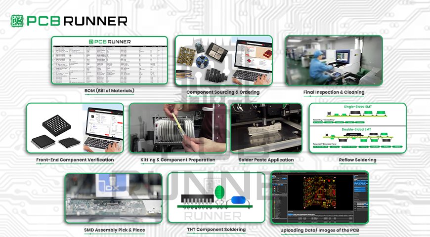
The entire process of assembly technology is captured in this diagram sequentially. Below are the steps on how it is performed: 

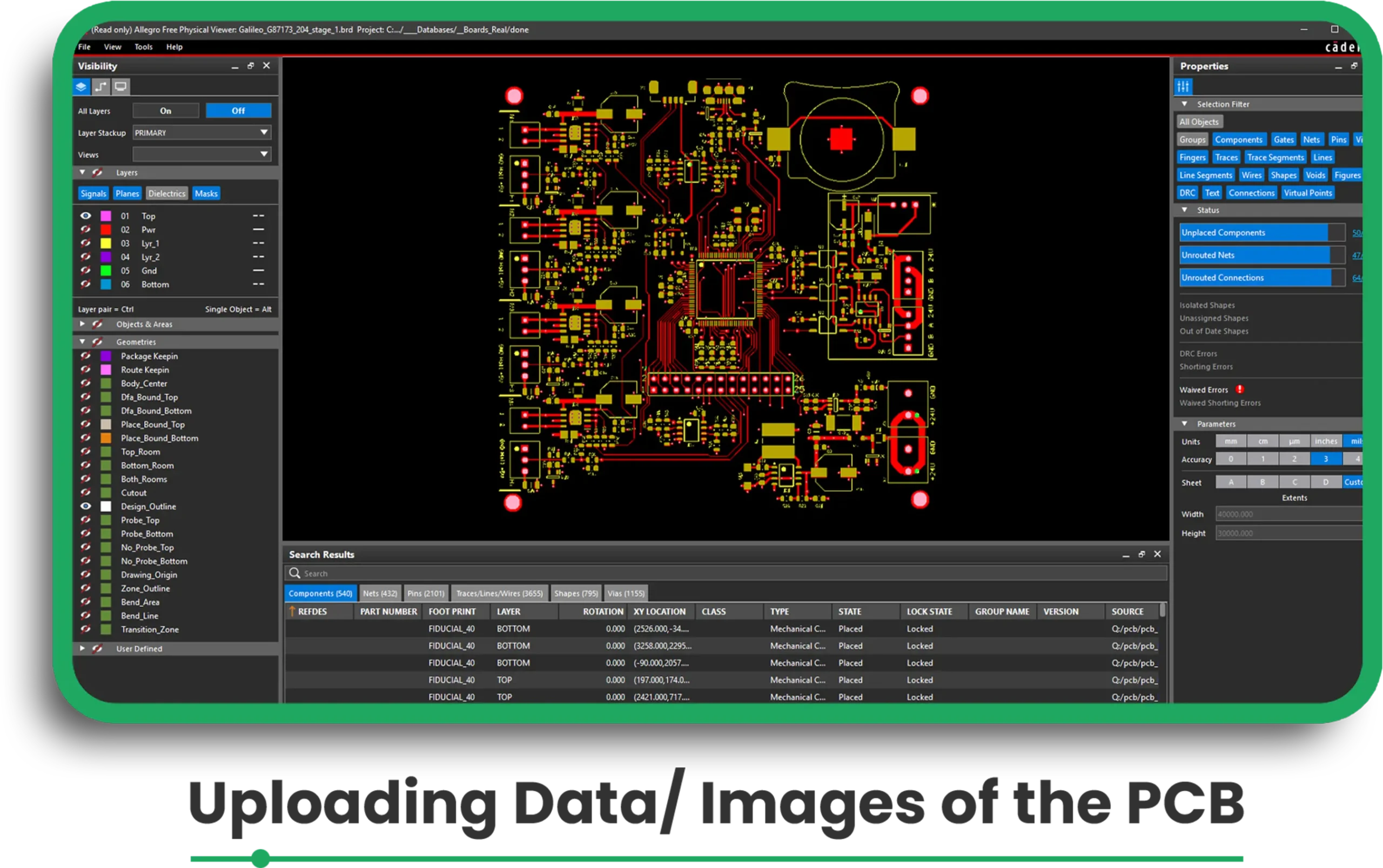
Step 1: Uploading Data/ Images of the PCB 

eC-smart tools such as the PCB Visualizer have enabled engineers to check their designs before the assembly phase commences. 

The company has to upload the images of the bare board for processing. 

Uploading data

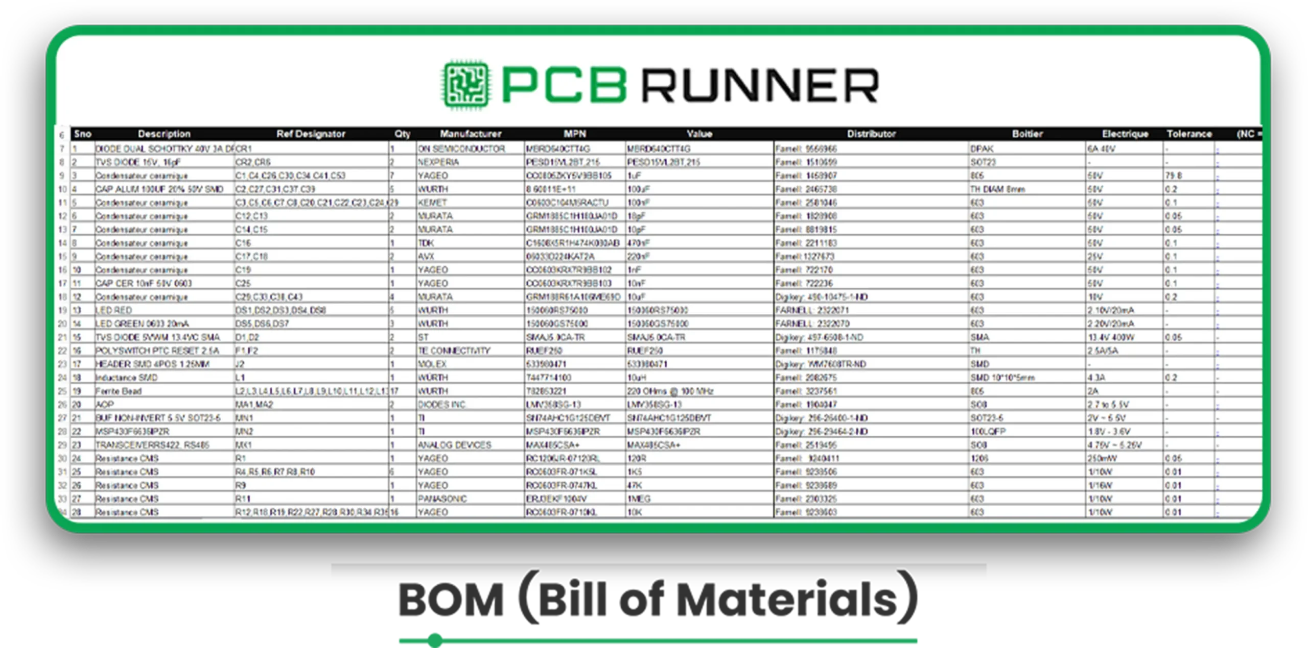
Step 2: Uploading BOM and CPL Files 

The BOM (Bill of Materials) includes all component items, such as part number, description, and packaging. 

The Component Placement List (CPL) describes the location of all components on the board. 

bom

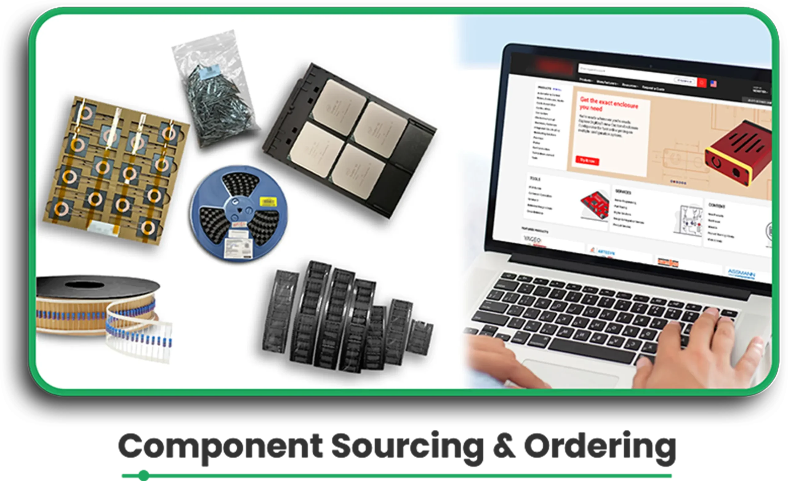
Step 3: Component Sourcing and Ordering 

An integrated system scans the BOM against the database of over 205,000 components to look for stock coverage. 

If components are not stocked, they need to be ordered from reputable suppliers through integrated APIs. 

Component Sourcing

Step 4: Front-End Component Verification 

For mounting, the correct placement, polarity, and type of package to be used against the PCB footprint are verified. 

Special requirements for mounting are determined and corrected in this phase.  

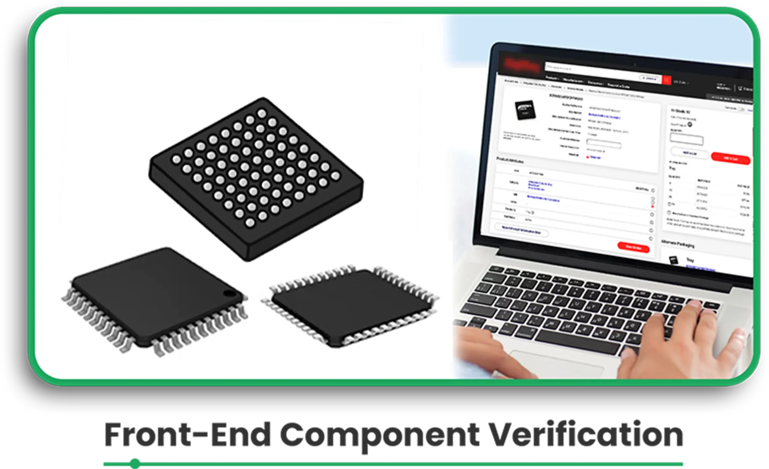
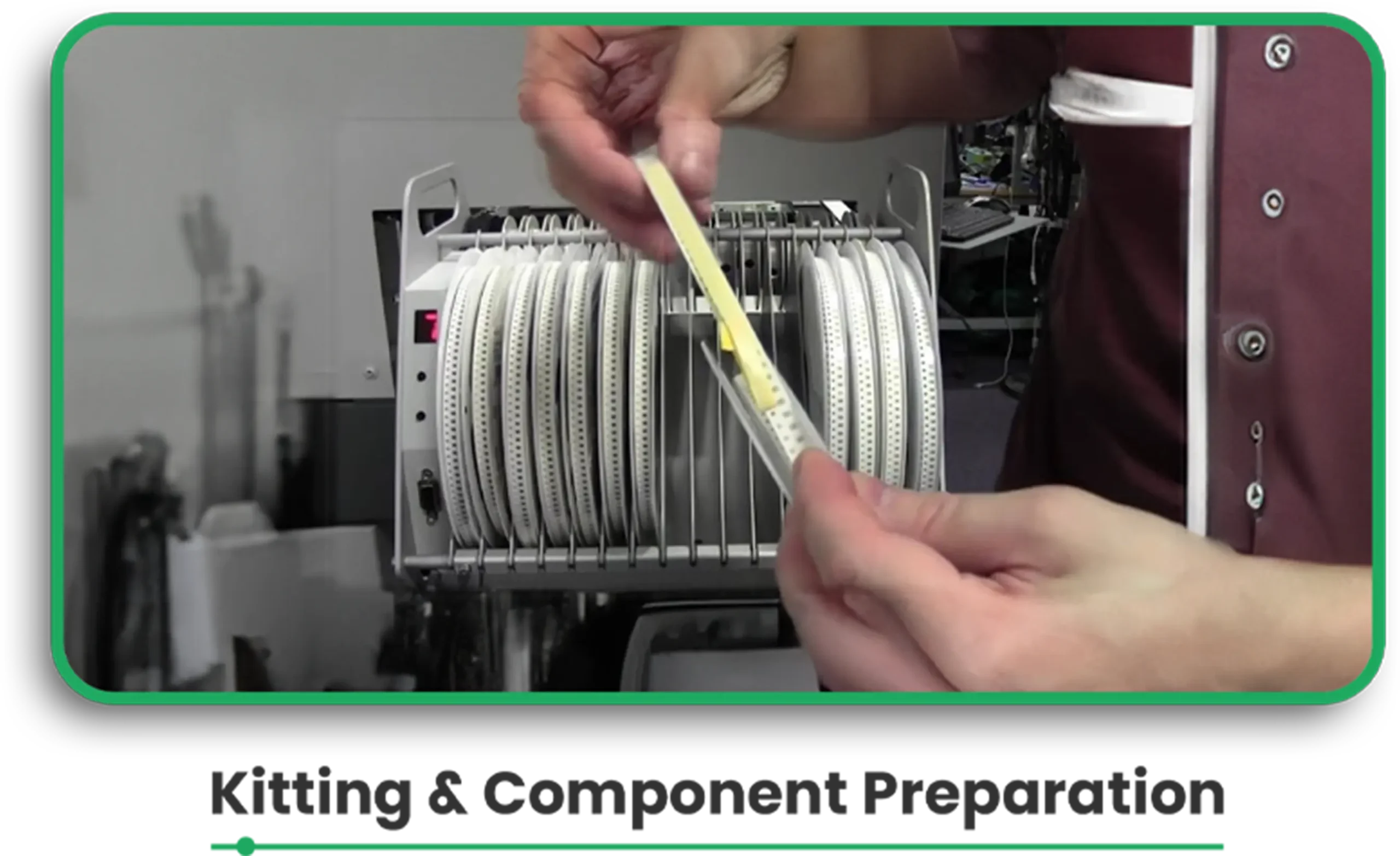
Step 5: Kitting and Component Preparation 

Items are arranged in feeders for better organisation, ensuring that they are loaded into the pick-and-place machines efficiently. 

Kitting & Component

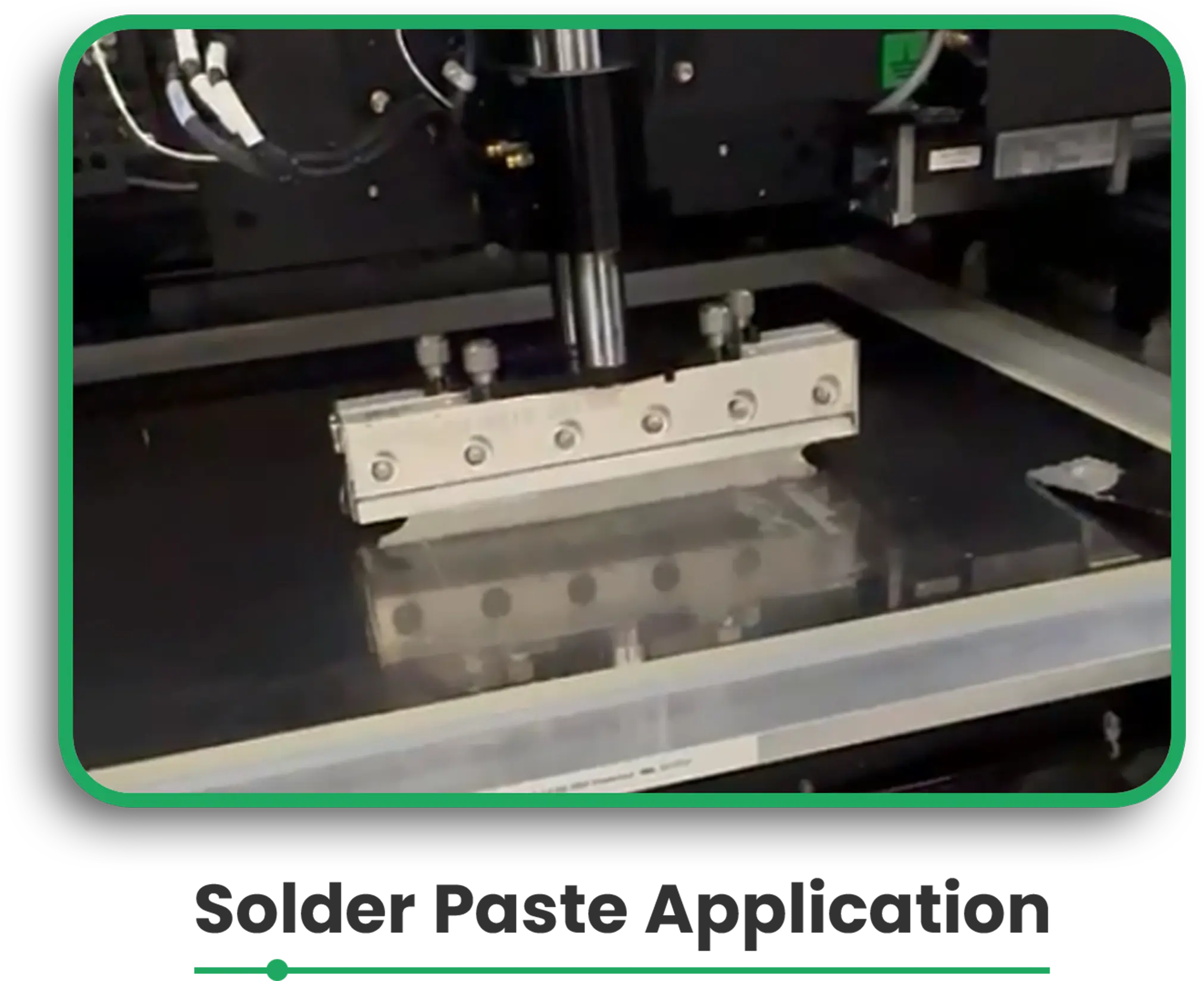
Step 6: Solder Paste Application 

Until this phase, jetting or SMD stencil printing performs solder paste application to the PCB surface. 

A solvent paste inspection (SPI) carries out the cure check to determine the paste’s adequacy for the ensuing procedure.

Solder paste

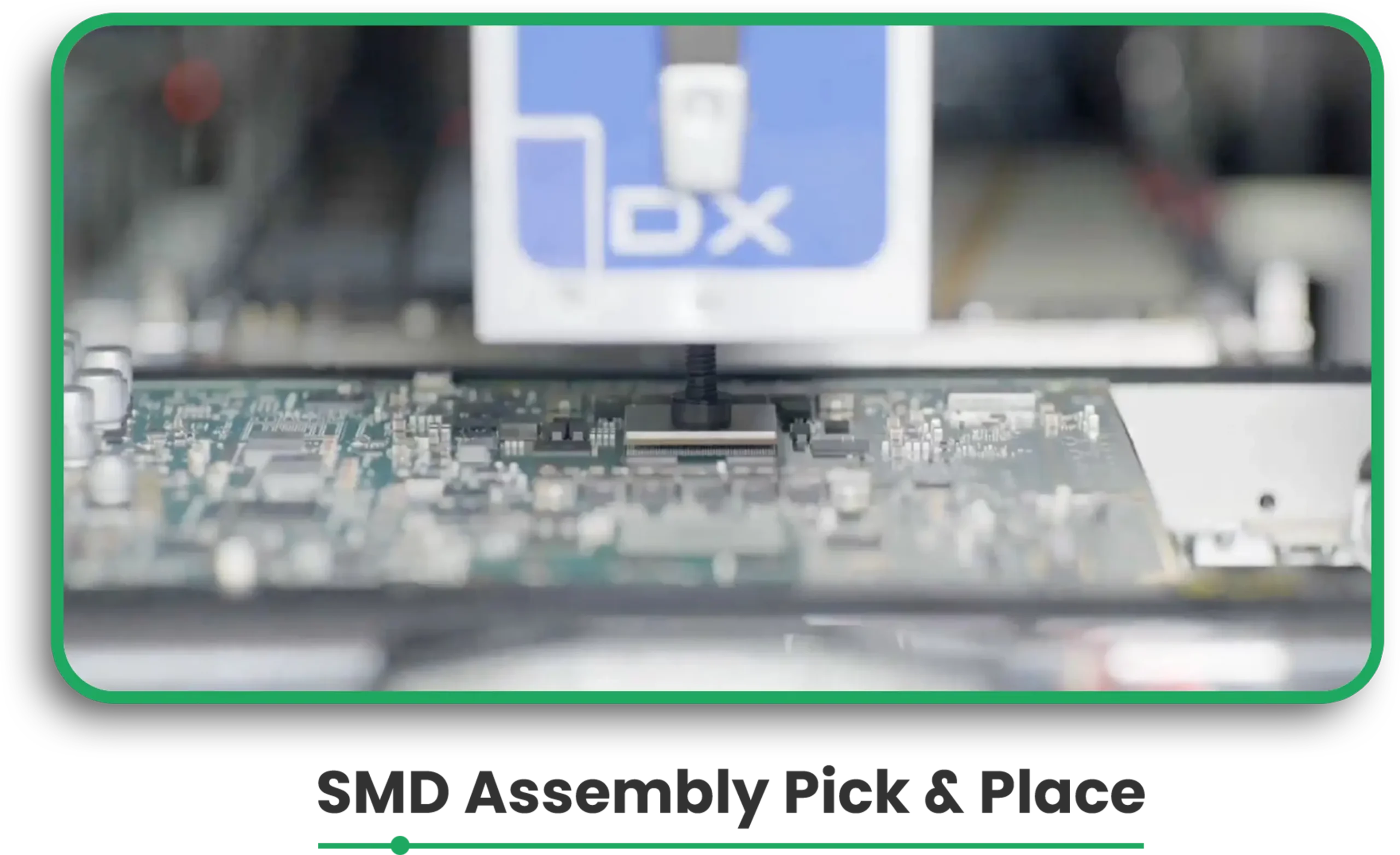
Step 7: SMD assembly: pick & place

SMD components are positioned on the board automatically by pick-and-place machines. 

Thus, vision cameras inspect components for their sizes and angle position. 

Smd assembly

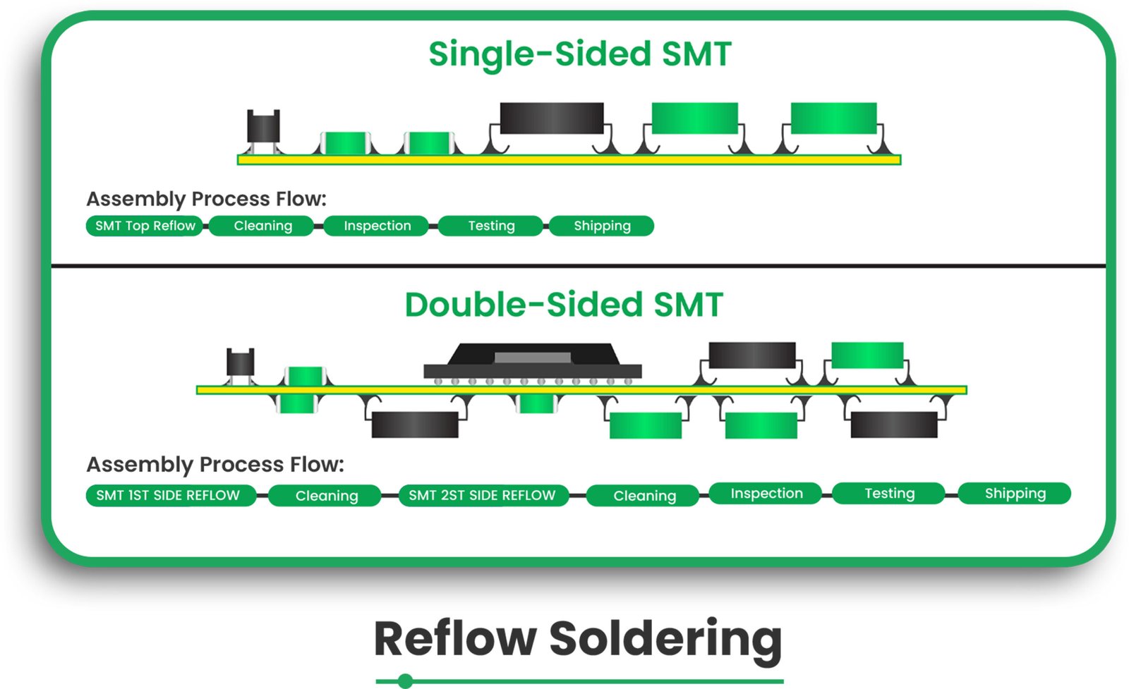
Step 8: Reflow Soldering 

The board is passed over a reflow oven, which helps melt the solder paste into a solid state, creating an inlet electrical connection to the components and PCB pads. 

Reflow Soldering

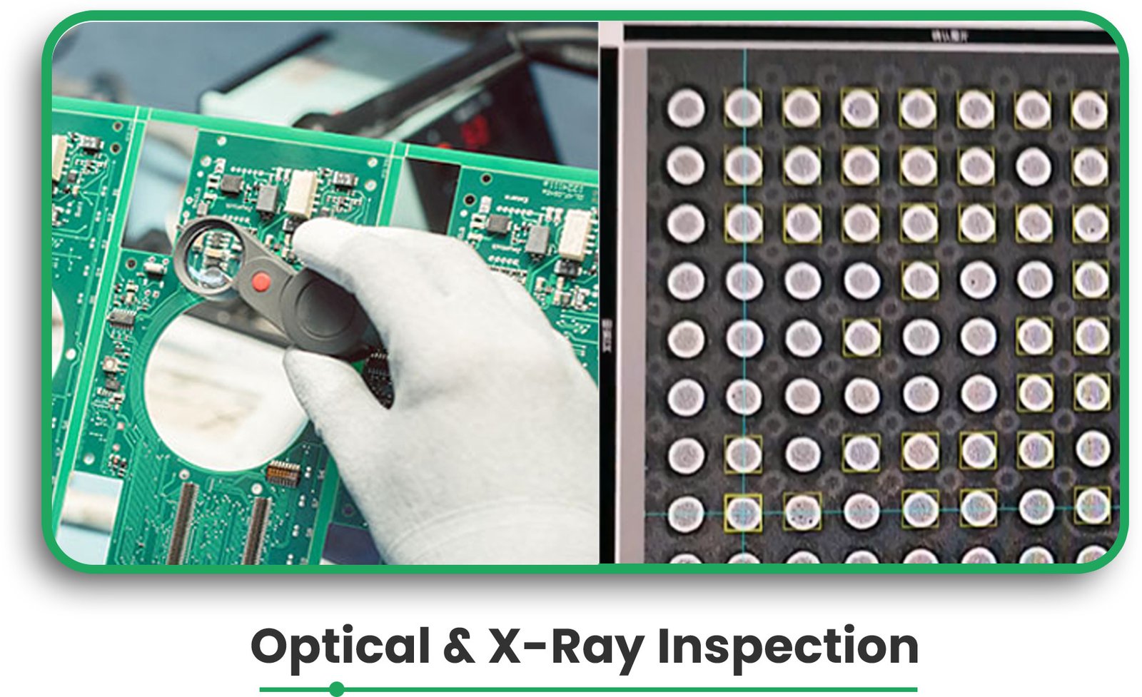
Step 9: Optical and X-Ray Inspection 

PixPect optical inspection scans the board for defects and correlates the image with properly scanned sheets. 

3D X-ray inspection can (with Nikon) detect concealed soldering connections and check the building quality of BGAs and LGAs components. 

Optical & x ray inspection

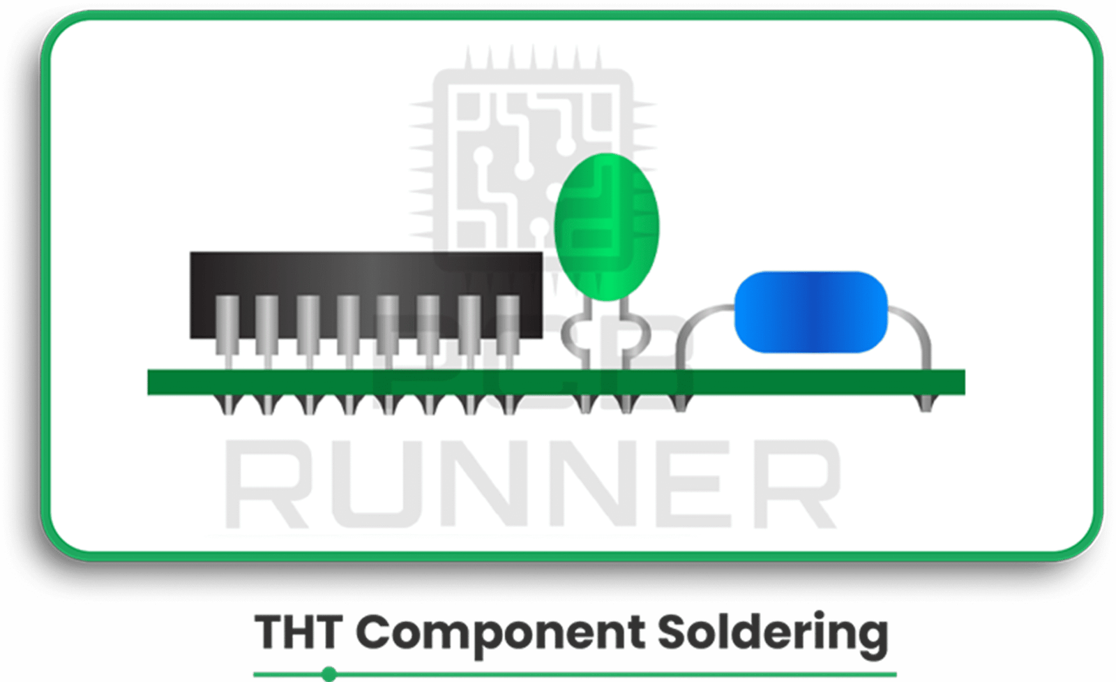
Step 10: THT Component Soldering 

Through-hole ones are assembled by means of selective soldering machines or manual soldering techniques

THT

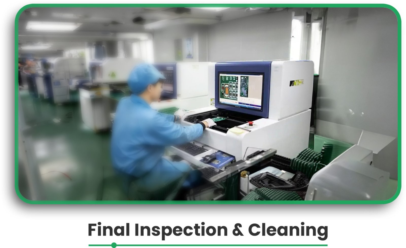
Step 11: Final inspection and cleaning 

The final inspection should make sure that the assembled board is suitable for the design specifications. 

Before shipping, the board is cleaned, and all defects are corrected. 

Final Inspection

Benefits and Application 

Step by step understanding of the PCB assembly enables one to undertake the following actions: 

  • Enhancing Quality Control: By ensuring validation checks at many processes, the chances of committing errors are greatly minimized. 
  • Facilitate AI Methods: Integrated systems like automated component ordering and solder paste dispensing help to achieve quick turnarounds. 
  • Guarantee Component Fitting: Employing tools like PCBA Visualizer guarantees that components are placed and fit in accordance with the PCB’s design. 

By following the above guidelines, accurate, high-quality PCBs are produced with shorter lead times, making it an essential resource for PC board manufacturers seeking efficiency in production.

Expert Insights:

The following information is mentioned in the PCB Design Tutorial by David L. Jones.”

Many people start designing a PCB by placing all the components where they think they’ll fit best right away. While this approach might work for simple circuits, it’s not ideal for more complex designs with hundreds of components and multiple functional blocks. 

The main reason is that you can quickly run out of “routing space,” which is the space needed to lay down all the tracks (connections). If you fix the positions of all components first and then try to connect them, you may find yourself stuck and unable to route some connections. On the other hand, if you space the components too far apart, you may end up with a large board that wastes space and increases PCB board manufacturing costs. 

An inexperienced designer’s board often has evenly spaced components but messy tracks and vias (holes for connections) crisscrossing all over. This kind of design might work, but it’s inefficient, unattractive, and more expensive to produce. 

The best way to start is by placing all the components on the screen first. If you’re using a schematic design tool, you can import the design into your PCB program to automatically place the components. If you’re only using a PCB program, you’ll need to select components from the library and place them manually. 

Once all the components are on the screen, you can assess whether they’ll fit within the size and shape of your board. If the fit is tight, you’ll need to position the components carefully to save space and keep the routing efficient. 

If you have plenty of space, you can be more flexible with your layout. However, if the components don’t fit at all, you’ll need to revisit your design and adjust. 

FAQs 

What files do I need for PCB assembly? 

To ensure smooth printed circuit assembly, you need to upload the bare board data, BOM (Bill of Materials), and CPL (Component Placement List)

What is the purpose of solder paste inspection (SPI)? 

SPI ensures that the correct amount of solder paste is applied to the PCB pads, which is critical for proper soldering and component attachment. 

How does the pick-and-place machine work? 

The pick-and-place machine automatically picks up SMD components and places them onto the PCB, ensuring precise component placement. 

What is selective soldering? 

Selective soldering is a technique for attaching through-hole components to the PCB. It ensures precise solder joints without affecting nearby components. 

Why is X-ray inspection necessary in PCB assembly? 

X-ray inspection is essential for checking hidden solder joints, particularly for difficult-to-inspect components like BGAs (Ball Grid Arrays) and LGAs (Land Grid Arrays). 

Conclusion  

The PCB assembly process involves a series of well-coordinated steps that ensure the final product is functional and high-quality. From design verification to component sourcing and final inspection, every phase plays a vital role in producing reliable PCBs. 

By understanding this comprehensive process, both engineers and PC board manufacturers can make informed decisions that lead to faster production times and more cost-effective solutions for prototypes and small series production.

In-Circuit Testing vs Functional Testing: Which One Is More Effective?

In-Circuit Testing vs Functional Testing

Once a PCB fabrication & PCB assembly is completed, quality and reliability testing are performed to ensure the final product’s functionality. Numerous methods are used for testing, two of the most popular being In-Circuit Testing and Functional Testing.
Though both of these testing methods are used to achieve quality control, their results, outputs, and mechanisms are different.

Understanding the differences between these methods allows manufacturers to select which one better fits their requirements. In this blog, we will discuss the merits and demerits of ICT and FCT and what scenarios they can be used for.

This blog will provide insights into the effects each of these testing methods has on the final PCB prototype and assembly’s performance and reliability.
From an experienced PCB engineer to a novice in the field, everyone will be able to comprehend which testing mechanism meets their needs and how reducing testing costs will increase product quality.

In-Circuit Testing vs Functional Testing
In-Circuit Testing (ICT):

Purpose: The ICT is used to look for breakages such as open connections, shorts, misaligned components, and incorrect component values on the PCB during circuit and component testing.

How it works: During the ICT, a custom “bed of nails” fixture is utilized to test various parameters of each board component by applying electrical signals to it and measuring its resistance and capacitance.

Beds of Nails Testing

Pros:

– Manufacturing defects can be located quickly and accurately

– The chance of assembling the parts on non-functional / X-Outs circuits gets low.

– It is suitable for mass production.

Cons

The need for unique test fixtures implies that these tests come with a significant initial cost.

It does not examine the PCB in actual operating conditions, which limits its scope.

Functional Testing (FCT):

Purpose: It functions by testing the PCB as a part of the final product in a box build assembly but in controlled alternative conditions. 

How Does It Work: A test fixture is applied that shows output readings, such as the assembly’s temperature, voltage, or frequency, allowing it to serve its purpose and also could be an indication on testing equipment with green/red leads.

Functional TestingPros:

-It allows do attempt of the final product to a detailed examination of the operative capacity and operating nature.

-The product is able to function in real-life conditions while being assembled, supporting the desired output considered by product designers.

Cons:

-Requires custom testing equipment to support high-end technology, which can be difficult to procure.

-It is a bit more costly due to the complexity of dealing with and ordering custom test fixtures, but the savings in time make it worth the cost.

Benefits and Application

Using Either ICT or FCT along with the correct testing method has plenty of benefits. Utilization of the correct testing strategy has its share of benefits. Using one or the other has some abnormalities on the testing side that should not hamper overall operation.  

In-circuit testing (ICT)

It aids in the detection of manufacturing anomalies like shorts or open connections. Therefore, it reduces the chances of the final product having flaws by enabling each element to be assembled appropriately. It is most beneficial in mass production when speed and accuracy in servicing are major requirements or concerns.

Functional Testing (FCT)

It is highly valuable in conditions where the board is of great use, and diagnostic functionalities are critical, such as consumer electronics, automotive testing, and medical emitters. It inspects whether the complete system is functional and ready to be used by checking whether all the parameters regarding a working system were met.

Expert Insights

The integration of In-Circuit Testing (ICT) and Functional Testing (FCT) has evolved to meet the demands of modern PCB assembly”. Modular circuit designers offer flexibility and scalability by allowing subsystems like the ICT module and the FCT module to be upgraded or replaced independently. This is useful for adapting to different testing requirements or technological advancements.

On the other hand, unified testing platforms consolidate both ICT and FCT capabilities into a single hardware/software framework. This approach simplifies configuration and operation, making it easier to manage the testing process. However, it may limit flexibility and expandability compared to modular architectures.

A hybrid approach combines the best of both worlds, offering both the flexibility of modular designs and the integration of unified systems. This balance ensures both scalability and streamlined testing operations.

Frequently Asked Questions

Which is better, functional testing or performance testing?

Both are important and better. Performance testing measures a PCB’s specific electrical characteristics which is also called as E-Testing (after fabrication is done), while functional testing evaluates its overall performance under real-world conditions which also called as Bootup Testing (after pcb assembly) Functional testing is usually more comprehensive and useful for confirming a product’s functionality.

What are the advantages of using in-circuit testing?

In circuit test is also known as ICT / NET List testing. The accuracy and speed of in-circuit testing can also detect assembly or manufacturing errors, such as shorts, open connections, or missing nets or stubs. The core advantage of running ICT test before PCB Manufacturing is that it allows to give surety to a manufacturer that there are no Nets shorting with guaranteed to be correctly routed and assembled without the application of power shorts so that the components will not be damaged.

What is a functional circuit test?

FCT Functional Test is used to check the electric parameters and specifications of the device. It checks the electrical parameters and specifications of a PCB assembly by functioning the device in a normal environment where the assembly is expected to work.

What are the 7 types of PCB testing methods?

  • In-Circuit Testing (ICT)
  • Functional Testing (FCT)
  • Flying Probe Testing
  • Automated Optical Inspection (AOI)
  • X-Ray Inspection
  • Boundary Scan Testing
  • Burn-In Testing

Conclusion

Both In-Circuit Testing and Functional Testing complement each other in terms of ensuring the quality and reliability of PCB assemblies. While ICT is suitable only for identifying defects, FCT, on the other hand, assesses the overall functional capability of a PCB when placed in real-life scenarios.

This is important because if manufacturers can effectively utilize all the pros and cons of each method, they will ultimately reduce the cost of the testing while improving the quality of the product.

Conductive Carbon Ink PCBs

A printed circuit board (PCB) with a carbon film conductive pattern is created by coating the PCB substrate with carbon-based conductive ink, also known as carbon ink, and curing it. As a result of the market’s persistent decline in PCB board production prices, carbon oil keys are increasingly being used in place of the more costly gold keys. For both single and double PCBs, carbon oil board is a comparatively popular surface treatment technique. The PCB is capable of long-term reliable operation through a battery of testing, including aging tests and inspections, as well as other technical procedures.

Benefits of carbon ink PCBs

PCB laminates made of polyester, FR-4, FR-5, PTFE, polyimide, and carbon ink are among them. Resolutions as fine as 100μm trace width and spacing can be proposed by the carbon ink. Jumpers, LCD contacts, and keyboard connections are typically utilized with the carbon contacts on the carbon ink PCBs. For carbon widths, 75% of the nominal value is needed. The carbon contacts are usually round and have a diameter of 2, 2.5, 3, 3.5, 4, 5, 6, 7, and 8 mm.

Carbon Oil Ink

1. The constituents of carbon oil

Carbon powder, hardener, and synthetic resin make up the majority of carbon oil. Adhesion is aided by synthetic resin, which functions as a carrier. The function of the hardener is to cure.
A conductive role is played by carbon powder (graphite powder can be added, although it is expensive).
To increase conductivity and reduce resistance, some vendors dilute the carbon oil with a small amount of silver foil.

2. The carbon ink’s resilience

Square resistance is a common way to express carbon oil resistance. There are two types of ohms per square centimeter that are used: Ω/cm² and Ω/□. Today, most providers consent to using Ω/□.

The resistance value of any square carbon film on the other side is referred to as square resistance, and it is correlated with the carbon oil’s composition and thickness. One can examine it by looking at the figure below.


Carbon ink PCBs rules and guidelines

In line with Ohm’s law:

R=ρ*L/S, where L is the length of the carbon oil, S is the side area, and ρ represents resistivity. Thus, if L=m, R=ρ*L/r*m R therefore equals ρ*r. The formula above shows that “Ω/□” can be used to describe the surface impedance when it is L=W, or when the length and width are equal. However, it needs to be specified at what thickness the “Ω/₡” value is. Suppliers often indicate ≤ 30Ω/□ at 15um or 25um.

3. The management of carbon oil resistance

The content and thickness of carbon oil are the sole factors that affect its resistance. Thus, we need to consider three factors in order to have a resistance requirement that is sufficient.

  1.  A reasonable square resistance carbon oil that meets the process requirements.
  2.  After printing, a suitable thickness (0.01-0.025mm) ought to be attained.
  3.  Baked at a temperature of 150°C to 170°C for 30 to 60 minutes, or 150°C for 15 minutes in an infrared oven.

High temperatures, lengthy operating times, and low square resistance are all present throughout the actual operation process. Selecting an appropriate temperature and duration without compromising the substrate is crucial.

Factors influencing the PCB carbon ink production quality

1. Design

The conductive coating and inner layer of insulation are created by screen printing, while the conductive carbon ink PCB is produced by an additive technique. In order to provide the illusion of joining the circuit’s upper and lower layers, the connecting disks are stacked. In this manner, the process of producing it just requires the addition of two printed graphic layers to that of a single-sided circuit board.

2. Material Selection for Screen Printing

1) Choosing conductive carbon ink for the isolation layer of insulation

Jumper wires are supported and insulated by the printed insulation isolation layer. The product’s quality is immediately reflected in this layer’s quality. High insulation is the guiding criterion for choosing insulation layer ink. As a result, the phenolic system’s insulating layer ink is typically selected.

2) Choosing an Ink with Carbon Conductivity

Good conductivity and a lower coefficient of friction—which can be improved with longer friction times—are characteristics of carbon-based conductive ink. It also has a reduced surface contact resistance.

Select carbon ink as the primary ingredient. Particles of carbon ink resemble spherical colloidal particles in form. Strong adsorption is produced by graphitized carbon ink’s high carbon content, very low resistivity, high conductivity, and wide surface area for separation. Its dispersion improves as a result of its microscopic particles, which also lead to improved wear resistance, greater variable area, reduced resistance, and extraordinarily high conductivity.

3. Control of the production process

In terms of production process control, the main points to be noted are as follows:

  • Control of screen-printing process methods
  • Screen printing plate.
  • The effect of curing conditions on resistance
  • The impact of the punching process
  • The influence of the surface treatment process

Carbon ink PCB is a material made of high-purity graphite sintered at high temperatures, with very high strength and hardness. Compared with metal materials, carbon plates have higher strength and advantages in high-temperature and high-pressure environments.

Benefits of PCBs with Carbon Ink

Printing on PCBs with carbon ink is eco-friendly. It won’t contaminate the soil, water, or air. Carbon ink circuit boards also provide excellent durability at a reasonable cost.

  1. Flexible: Carbon ink printed circuit boards (PCBs) are particularly well-suited for applications requiring flexible circuit boards, such as wearable technology, sensors, and flexible electronic items since they can flexibly adapt to bending, folding, and unusual shapes.
  2. Low cost: Because carbon ink is a relatively inexpensive and simple-to-print substance, the manufacturing cost of carbon ink printed circuit boards (PCBs) is lower than that of typical copper foil circuit boards.
  3. Environmental protection: In compliance with regulations pertaining to environmental protection, the carbon ink ingredients used in carbon ink PCBs are usually non-toxic, innocuous, and biodegradable.
  4. Electromagnetic shielding: The carbon ink layer efficiently reduces electromagnetic interference and crosstalk due to its outstanding electromagnetic shielding ability.

Read More: PCB Standards and Heavy Copper Thickness 

Applications for PCBs using Carbon Ink

Applications for carbon ink PCB include RF shielding, automobile vehicles, keypads, remote controls, industrial engine control, calculators, phones, computers, TVs, and VCR typewriters. It is primarily used to provide a protected contact surface for switches.

One of the main factors influencing the reduction of PCB manufacturing costs is carbon ink, sometimes referred to as conductive carbon ink.

In terms of resilience, dried carbon ink is often sufficiently durable to bear over a million keystrokes on a keyboard or over a hundred edge connector insertions without exhibiting wear or increased resistance.

Characteristics of carbon ink

The three characteristics of carbon ink are its viscosity, thixotropy, and liquidity.

1. Viscosity

The internal friction of a liquid is called viscosity. It is also known as the liquid’s mechanical resistance among its many layers. In a thicker liquid than in a thinner liquid, its strength is always greater. It has been noted that viscosity is greatly influenced by temperature.

2. Thixotropy

The physical attribute of a liquid that allows it to regain its original viscosity or structure is known as thixotropy. It facilitates the liquid’s internal structural reconstitution. Screen printing is thought to work better using thixotropic ink.

3. Liquidity

The amount of outside force acting on ink is its liquidity. It is the most crucial component of printing. It is viscosity reciprocal. In order to provide even coverage across the copper button pads, carbon ink circuit surfaces need to have high printing qualities and good viscosity stability in warmer regions.

Screen printing is a straightforward process for printing carbon ink on PCBs. Engineers can save money on carbon ink PCBs because of the simple plating procedure and less expensive ink.

Conclusion

When it comes to flexibility, customization, and quick prototyping, carbon ink circuit boards are a revolutionary step forward in electronic design and production that standard rigid PCBs just cannot match. The future of electronics across industries is being shaped by the versatility of carbon ink circuit boards, which are being used in wearable electronics, medical devices, and Internet of Things applications. Even if there are factors like conductivity and durability, they can be efficiently addressed with careful design, skilled manufacture, and a full grasp of the advantages and disadvantages of the technology. Carbon ink circuit boards are a monument to the creativity that propels the electronics sector forward as technology advances.

FAQ’s

Why and Where to Use Carbon Ink Technology?

Printed circuit boards using carbon ink are frequently utilized in the following applications:

  •  Automobile Vehicles
  •  RF Shielding
  •  Keypad Keyboard
  •  Remote Controller
  •  Industrial Engine Control
  •  Welding Equipment

The use of rubber keypads, which are frequently used in garage door controllers and television remote controllers, is one area in which Carbon Ink PCBs shine. A standard conductive rubber keypad has a switching centre surrounded by angled webbing. The webbing stretches and responds tactilely when the switch is pressed. The webbing goes back to its neutral state as soon as the switch is not compressed.

How does it apply to PCB during manufacturing?

Carbon-based ink: A printed circuit board (PCB) that uses carbon ink as a conducting substance is referred to as a PCB. To form conductive traces or patterns on the PCB surface, carbon ink is a mixture of carbon particles and a binding agent. To achieve high-density wiring, conductive carbon ink designs are applied in one or two layers to a single-sided printed circuit board using a straightforward screen-printing technique. Printed conductive patterns find application in resistors, key switch contacts, electromagnetic shielding layers, and other applications that align with the current trend of electronic product shrinking, lightweight, and multi-functionality.

Why Us?

PCB Runner offers conductive carbon Ink manufacturing based on design requirements, we provide reliable & good quality circuit boards and can handle carbon paste/ink on surface pads. Submit your Gerber files at https://www.pcbrunner.com/free-pcb-quote/ or do reach out to our team offline at engineering@pcbrunner.com or sales@pcbrunner.com for your current or upcoming project’s needs.


PCB Standard & Heavy Copper Thickness

A new trend in the printed circuit board business, Heavy Copper, and Extreme Copper Printed Circuit Boards, is being tapped into by an increasing variety of power electronics products. The majority of PCBs that are sold commercially are made for low-voltage/low-power applications, and their copper traces and planes are composed of copper weights that range from 1/2 to 3 ounces per square foot. Copper weights for a hefty copper circuit can range from 4 to 20 ounces per square foot. Extreme Copper refers to copper weights that are above 20 oz/ft2 and can reach up to 200 oz/ft2. We’ll be talking mostly about heavy copper thickness.

Heavy copper thickness in PCB manufacturing process 

Standard printed circuit boards are created by combining copper etching and plating techniques, regardless of whether they are double-sided or multilayered. Initially, circuit layers are made of thin copper foil sheets (usually 0.5 to 2 oz/ft2) that are etched to remove excess copper and then plated to give planes, traces, pads, and plated-through holes more copper thickness. The circuit layers are assembled into a comprehensive package by laminating them onto an epoxy-based substrate, like polyimide or FR4.

The production process for boards with heavy copper circuitry is the same, but specific etching and plating methods, like differential etching and high-speed/step plating, are used. In the past, thick copper-clad laminated board material was totally etched to create heavy copper features. This resulted in uneven trace sidewalls and unacceptably high undercutting. The combination of plating and etching has made it possible to manufacture hefty copper features with straight sidewalls and minimal undercut because to advancements in plating technology.

The Advantages of Heavy Copper PCB

  • Better thermal performance: During the manufacturing and assembly procedures, heavy copper printed circuit boards (PCBs) can tolerate numerous temperature cycles.
  • Greater current carrying capacity: PCBs made of heavier copper have larger current capacities and better electrical conductivity. The current carrying capability can be increased by widening the copper trace, and even higher current loads can be supported by thicker copper traces.
  • Enhanced mechanical strength: PCBs made of heavy copper have stronger connections and plated-through holes, which guarantees the board’s structural integrity and increases the electrical system’s resilience to voltage.
  • Outstanding dissipation factor: PCBs made of heavy copper work well with big power-loss components. These PCBs have the ability to efficiently disperse heat and stop electrical systems from overheating.
  • Good conductor: Heavy copper PCBs are useful in the manufacture of electrical items because they are good conductors. They assist in joining different boards so that currents can be transmitted.

Applications for PCBs Made of Heavy Copper

Because heavy copper PCBs are widely used in the following industries, their popularity is growing:

  • Military: Radar, weapon control, and surveillance systems.
  • Rails Tracking: Rail track system and signal transmission system for the automotive sectors.
  • Power distribution: High power rectifiers, power grid switching systems, overload relays, and excitation systems for power regulators.
  • Transportation: Traction converters, power line monitors, and power converters for railroad systems.
  • Industrial controls: Surge protectors, protection relays, welding equipment, safety, and signal systems. 
  • Renewable Systems: Control panels for hydroelectric power facilities, energy storage, power grid backup, and power converters.

 Services offered by PCB Runner include PCB Assembly (SMT), Electronics Module Sales, CNC Machining, PCB Prototype & Batch Production, and more. We are dedicated to satisfying the demanding demands of international manufacturers across many industries with regard to electronics quality, delivery, affordability, and other matters.

Heavy Copper Thickness PCB Design Guidelines

The following are some important design factors for PCBs made of heavy copper:

Layer Assembling

  • To reduce warpage, place thick copper layers close to the board’s core.
  • Avoid positioning outer layers adjacent to one another as this can worsen registration problems.
  • For stability, rotate the direction of the fiber weave by ninety degrees between neighboring dielectric layers.

Part Location

  • To ensure solder mask coverage, make sure there is enough space between plane layers.
  • Take into consideration component shadows that fall on inner copper layers.
  • Inspect drilled holes for exposed copper.

Temperature Control

  • To serve as heat spreaders, place heat-generating components on top of thick copper layers.
  • Provide many vias to distribute heat to the interior planes underneath heated components.
  • Elevated Current Pathways
  • For high-current lines, use copper pouring or polygons rather than routing several parallel traces.
  • For heat dissipation, place next to plated thru-hole vias.
  • The use of filled vias should be restricted since, in comparison to hollow vias, they hinder heat transfer.
  • Solder masks should be kept free of holes and countersink-filled vias.

Panel and Tooling

Give ample room for manufacturing and assembly tolerances. Consider warpage, stretching, and shrinkage of the cloth. For simple tooling, use fiducials and test coupons on the panel.

DFM Evaluation

During the design phase, ask the fabricator for DFM feedback.

In particular, look into manufacturability with regard to heavy copper tolerance concerns.

Getting in touch with the PCB maker early on streamlines the design process and helps to prevent problems during the prototype.

Finding the Right Heavy Copper Partner

Make sure the PCB manufacturer you choose for your heavy copper boards satisfies the following requirements.

Checklist of Capabilities

  • Lamination thicknesses of 2 oz, 3 oz, 4 oz, and so on are available.
  • PTH filling: epoxy plugs, conductive ink, and copper
  • Preferred registration accuracy is ≤ 0.003″.
  • Etching with fine lines: < 4 mil line/space
  • The thickness of plating: ≥ 2.5 mils copper in holes
  • Gaps to be filled by sectional plating after etch AOI examination – 5+ high-resolution cameras.

Standards and Licensure

  • Shop floor processes in accordance with IPC 6012 Class 3
  • ISO 9001 certified
  • UL or TUV-approved facilities
  • Qualification testing- vibration, shock, and thermal stress

Technical Proficiency

  • Familiarity with intricate copper designs
  • Support for Design for Manufacturing (DFM)
  • Simulated plane currents and thermal analysis
  • Comments on dependability, stacking, and layout

Active Prototyping

  • Minimal NRE expenses
  • There are no minimum order requirements.
  • Compact panel or array sizes
  • Simple 2-4 layer constructions can be completed in 24 hours.

Examine manufacturers carefully based on these factors prior to selecting your heavy copper PCB supplier.

Read More: PCB Component Placement Guide – Everything You Should Know For Effective PCB Assembly! 

Conclusion

Applications with large current loads, demands for thermal performance, and requirements for power integrity are made possible by heavy copper PCB technology. Although the thick copper layers increase reliability, strict process controls are required during fabrication. The benefits of heavy copper PCBs in your product can be realized by closely collaborating with the PCB manufacturer throughout the design phase and adhering to layout specifications. Heavy copper fabrication calls for specific accuracy and knowledge, thus working with a reputable manufacturer that offers design reviews and qualification testing yields the best results.

FAQ’s

When is the high copper thickness required?

Applications that need power conversions, thermal dissipation, high power distribution, and planar transformers require PCBs with high copper thickness.

Are there any trace width & and spacing restrictions while using high coppers?

High signal count parallel buses or very fine pitch BGAs are examples of PCB footprints used in high-density designs that may call for trace widths as thin as 2.5 mils and unique via types such as laser-drilled micro-vias with diameters of no more than 6 mils. On the other hand, some high-power designs may call for thicker ounce pours than usual and very big traces or planes that consume a complete layer. Applications with limited space may call for extremely thin boards with multiple layers and a half-ounce (0.7 mil) maximum copper pour thickness.

Can high copper traces impact power noise?

Copper traces on PCBs are crucial. Heavy copper can be used to narrow the track width in high-power printed circuit board production while maintaining the same current capacity. The circuit board’s area of occupancy decreases with decreasing PCB track width. In addition, copper busbars for high power and high current can be welded to PCB pads. 

Why Us?

PCB Runner offers Heavy copper clads manufacturing based on high current design requirements, we provide reliable & good quality circuit boards and maintain the required high voltage calculations. Submit your Gerber files at https://www.pcbrunner.com/free-pcb-quote/ or do reach out to our team offline at engineering@pcbrunner.com or sales@pcbrunner.com for your current or upcoming project’s needs.


Difference between Counterbore and Countersink

The goal of both counterbores and countersinks is to enable the head of a screw or other fastener to rest flush with or slightly below the surface of the material they are placed into. The angle at which the bigger hole is drilled separates them from one another. A counterbore is drilled straight into the material, leaving a level bottom between it and the narrower inner shaft, while a countersink’s bigger hole tapers at an angle.

Counter Bore

Except for a handful, the information required for each class is nearly the same. Since a counterbore is always drilled straight down without a taper, the angle is not necessary to know.

counterbore and countersink bits differences

Countersink

We need to know the intended angle because a countersink is not drilled straight into the material. For those who are interested in mathematics, you have probably noticed that the angle and the major hole diameter make a triangle. The angle, major, and main diameters dictate the depth to which the countersink will be drilled, yet stating your anticipated depth is a useful way to verify your expectations.

  • Which way around is the sink on the board? Above or Below?
  • Is plating or not plating appropriate for the hole walls?
  • The hole’s small inner shaft’s completed diameter. (First Drill)
  • Major Diameter: the hole’s final surface diameter
  • The tapered drill’s angle.
  • Depth at which the countersink should be drilled.

Differences between counterbore and counterskink drills in PCB

Important Distinctions Between Counterbore and Countersink Holes

Although hardware can be positioned flush on the board surface with both hole types, there are some significant variations that affect how they are used:

1. Shape of a Hole

The form of the hole is the main distinction. Counterbores have straight cylindrical walls, whereas countersinks have conical shapes. This affects the fastener’s flushness against the board.

2. Size of Top Opening

In a similar vein, the two holes differ in the size of the top opening. A countersink’s top taper gradually from the entire hole width. A counterbore is matched in diameter to the fastener and has a broader concentric cut on top.

3. Walls That Are Vertical

Counterbores have vertical walls, and countersinks have inclined side walls. Fasteners have greater shear strength when the walls are vertical.

4. Width of Bottom Opening

A counterbore’s bottom hole aperture is larger than a countersink’s of equivalent size. This increases the design’s versatility in terms of fastener size selection.

5. Material Elimination

In order to make a countersink, more material is removed from the PCB. Counterbores preserve the strength and substance of PCBs.

When to Use PCB Counterbore and Countersink?

Now that we have a fundamental understanding of counterbore and countersink holes, let’s examine their applications in printed circuit boards.  These fittings can be used on a printed circuit board, even though they are typically meant for stronger materials like metal and wood.  A PCB has holes, just as most circuit boards, and how each hole is drilled counts.
 There are screw holes in some of these holes that are utilized to attach the PCB to an application.
 The sort of screw you can use to drill countersunk or counterbore holes into the PCB depends on what kind of screw is available. Instead of saving space or choosing a smoother design, use counterbore holes if you need a more stable PCB installation.  The screws from them will provide a more stable attachment because these holes are typically big enough to fit socket fixtures.  However, if you’re looking to save space, opt for a countersink hole.

For PCBs, which is better?

Knowing the main distinctions between counterbore and countersink holes is essential to determining when to utilize one over the other during PCB assembly.

The substance you’re drilling into frequently determines which technique you should use. As previously noted, countersinking is frequently recommended when working with wood to prevent overtightened screws from damaging the material.

Most manufacturers will utilize the counterbore approach instead of countersinking during PCB assembly to prevent needless damage to the PCB since countersinking necessitates using an angle and additional depth from the drill. Additionally, countersinking necessitates greater tools and materials, which could prolong the production process and endanger the board.

A ground or earth terminal, which is essentially a physical connection to the earth and serves as a secure return point to drain excess current, can be used to establish a connection through counterboring.  Counterbore holes are also the finest option if you need to mount your PCB more securely. The screws from them will provide a more stable attachment because these holes are typically big enough to fit socket fixtures.

Principal Uses for Each Type of Hole

Countersink and counterbore holes have distinct uses because of their characteristics.

  • Typical Applications for Countersunk Holes
  • Installing flush screws on PCBs’ outside surfaces
  • Allowing low-profile bolt heads that must be flush with the surface of the board
  • Creating a sleek surface for aerodynamics on exposed external PCB layers
  • PCB mounting on thin aluminium covers or panels

Usage of Counterbored Holes in Common:

  • Fasteners for mounting machines that require a high shear strength
  • Letting spacers or washers rest flush against the PCB surface
  • Allowing bigger fastener heads to be accommodated with less material removal
  • Supplying the highest strength possible for screw connections at heavy load
  • Properly assembling internal PCB layers while reducing surface defects

Counterbores offer stronger screw joints, especially for internal PCB layers that are hidden, but countersinks are often better for applications where aerodynamics and aesthetics are important considerations.

Design Factors to Consider When Choosing a Hole Type

Engineers should consider the following aspects when designing a PCB layout and choose between countersunk and counterbored holes:

Sizes of Fasteners

More fastener heads can be used in counterbores than in countersinks of the same size.

Board Space Available

Because of their tapering design, countersinks require extra space.

Location of the PCB Layer

Counterbores work better for internal layers, whereas countersinks maximize outward layers.

Requires Shear Strength

Compared to countersunk holes, counterbores offer stronger screw joints.

Exposure to Environment

For external PCBs, countersunk holes enhance weatherproofing.

Priorities for Aesthetics

The surface finish is smoother with countersunk holes.  It will be easier to guarantee that the hole type chosen offers the appropriate functionality for the application if these factors are considered early in the design process.

 Drilling and completing Compare Counterbored vs. Countersunk Holes

  A functional, dependable PCB requires appropriate drilling and finishing procedures after the hole type has been chosen. The following are some recommended procedures:

Cutting Countersink Holes

  • Use a countersink drill bit that is specifically designed for the screw size. The correct angled hole cannot be created with standard twist bits.
  • To prevent breaking through the bottom layer or tapering too shallowly, precisely adjust the drilling depth.
  • When you get close to the bottom, don’t push too hard to prevent drill walking. Reposition and back off if there is a walk.

How Counterbores Are Drilled

  • A normal straight hole should be drilled first using a twist bit with a minor diameter.
  • Next, cut the shallow counterbore ledge to the required depth using a bigger bit.
  • When counterboring, support the board with a stiff backer to avoid a tear-out.

Finishing  Holes

After drilling, gently deburr the margins of both types of holes to prevent solder mask damage. Further polishing of countersinks with abrasive cones may be necessary to enhance fastener fit.

Proper drilling and finishing will result in smooth holes sized exactly right for the specified fasteners. This eliminates screw damage during assembly and offers reliable performance.

How to take dimensions for a Counterbore and Countersink

To account for the head of the flathead fixtures—which may be bolts, rivets, screws, or other similar objects—the angular sides of a countersink are recessed.

When drawing, the diameter, depth, and included rise of a counter-drilled hole are also provided, together with the surface diameter and angle.  The head of the fastener can rest in the recessed area of the counterbore’s flat-bottomed, cylindrical section.  When drawing and dimensioning this, the diameter, depth, and corner radius are provided and specified. In certain cases, the center can be substituted for the remaining shaft’s thickness when determining dimensions.  Either a rectangular or polar coordinate form could be used to size both holes.

Conclusion

To attach to various materials, counterbore and countersink holes are used with matching screws. It is possible, albeit uncommon, to use this as a print circuit board fixture. As we’ve seen, a counterbore is more cylindrical than a countersink, which is a hole with a cone form. This article has emphasized the distinctions between a counterbore and a countersink, as well as the parallels between them, their definitions, and how both holes function. Since the terms counterbore and countersinks can be used interchangeably, they refer to the same kind of screws that fit into both a counterbore and a countersunk hole. Additionally, we have seen how they differ in their manufacturing process by employing distinct drill bits for every kind of hole.

Why Us?

PCB Runner offers a proposed array based on the individual board requirements; we make it less hassle for the layout designer to step & repeat the PCB and supply us with panelized Gerber. Submit your Gerber files at https://www.pcbrunner.com/free-pcb-quote/ or do reach out to our team offline at engineering@pcbrunner.com or sales@pcbrunner.com for your current or upcoming project’s needs.

 FAQs

  • What minimum angle do we need to maintain for Countersink?

The hardware being used determines the countersink’s angle. Although it doesn’t have to match precisely, the hardware should have at least 50% contact with the countersunk hole. For hardware that is metric, the usual countersink angle is 90°, and for hardware that is imperial, it is 82°. We provide both perspectives in our sizes.

  • Can counter holes be plated for ground connections?

Plated is the best option if the screw is used to ground the board (such as PC motherboards) since it has numerous tiny vias radially surrounding the hole and the top, bottom, and internal ground plane connected together. The vias don’t have any heat relief. The vias make sure that the top and bottom pads are firmly attached to the ground plane, even in the event that the screw thread damages the hole plating. If not, it isn’t really important.

  • Does it cost extra in manufacturing?

However, as Scott Seidman points out, it can increase the cost of the board if there aren’t any other unplated holes in it. The type of lock washer or screw you put on the PCB may depend on whether or not there is a pad and how the pad is finished after assembly because solder has a propensity to flow cold. If the board is multilayer, there should be a lot of space between unplated holes and non-connected internal planes because you don’t want the screw shorting to (say) an internal power plane and the thread can damage the internal surface (people sometimes drill out holes that don’t quite match the mating surface).

Read More: How To Solve The Common Problems During Edge Plating In PCB Assembly? An Expert Guide

Solving Common Issues in Edge Plating PCBs Tips and Tricks


Edge Plating:

In the PCB industry, edge plating is also referred to as metalized edge plating, border plating, plated contour, side plating, and castellation. The PCB board’s edges are encapsulated by the electroplating coating, which extends from the top to the bottom surface. PCBs can have their single-axis or multi-axis edges plated. Frequently used to enhance chassis grounding for signals and EMI shielding for high-frequency designs.

Purpose of Edge Plating:

Using PCB plating, printed circuit boards can be better protected against a number of vulnerabilities. The edge plating can assist in the following four primary areas:

1. Signal and power integrity:

The board’s power and signal integrity will both be enhanced by EMI reduction. High-speed electronics will benefit from extra shielding and better current-carrying capabilities due to the expanded grounding provided by the edge plating.

2. Electromagnetic adaptability:

The current flowing between the ground and power planes on multilayer circuit boards may cause electromagnetic interference (EMI) at their edges. The circuit board may surpass the EMC criteria it is designed to fulfill as a result of this interference’s potential to radiate outside of the system. The metal plating barrier that surrounds the board’s edges stops the electromagnetic interference (EMI) from radiating.

3. Thermal dissipation:

As signal rates rise, circuit boards have the potential to produce significant amounts of heat. In order to transfer this heat uniformly throughout the board, thermal vias are usually used to route it into an internal ground plane. Heat can easily escape the board through the metal edge since the ground plane is attached to the edge plating.

4. Structural reliability:

A circuit board’s strength and stiffness are reinforced by the addition of metal on its sides. Regular use reduces the likelihood of physical damage to the boards. Additionally, the PCB’s metal sides offer superior support when sliding the board into the intended electronic systems’ metal frames and casings. Additionally, edge plating will shield the PCB from unintentional physical harm while handling or use.

PCB edge plating in assembly process

PCB Edge Plating Layout Guidelines

A few factors the designer should be aware of. A metal strip on the surface layers is first needed for the plating to bond with. In order to leave the metal strips exposed for plating, the designer must not only mention them in the layout data but also remove the solder mask from that region. Arranging the internal plane layers’ configuration is a crucial aspect of design.

It is necessary to move the power plane’s boundary away from the board’s edge, even though the ground plane is often attached to the edge plating. Any possibility that the power plane will make contact with the PCB edge plating during manufacturing and result in a direct power-to-ground short will be eliminated by pulling back the power plane boundaries.

The manufacturing drawings are the means by which PCB designers convey their intention for the edge plating. The sides of the board that must be plated, how the edge plating overlaps with the metal strips on the surface layers and the kind of plating and surface finishes needed must all be specified in the documents. A reputable PCB manufacturer can assist you in making these choices. 

PCB Edge Plating DFM Guidelines

Alongside the common board plating procedures, edge plating—also referred to as rout plating—occurs to denote the partial or total depanelization that takes place prior to the metallization process. This is less of an issue in single-edge plating, although partially routed boards may still include tabs in the panel that serves as just fasteners connecting the routed edges to the panel as a whole. Depending on when depanelization is to take place, these tabs must strike a compromise between ease of removal and durability because they are only meant to be temporary throughout production operations.

The following are some main points that should be kept in consideration while doing DFM of plating

  • The thickest point of the tabs between the board and panel should be about 2.5 mm or 100 mils. For better adhesion, the tabs on the substrate will be thicker.
  • To avoid exposure during de-tabbing, artwork surrounding the tabs on both the outer and inner layers should be free of metal. Set a minimum as your goal. There is a 25mm/10 mil gap between the copper layer features and the tabs.
  • Tabs may be solid for removal after manufacturing, or they may have mouse bites for a less rigorous breakup after assembly.
  • Generally, tabs are placed every 50 mm or 2 inches along routed edges; however, more frequent placement may be necessary for extremely thick or thin panels or those with less mechanically robust substrates.
  • The edge plating will wrap around the routed edge to the other side of the board for optimal adhesion. The edge plating needs to be at least 0.4 mm/15 mils beyond the edge, with a gap of 2.5 mm/100 mils between it and any other plated edges and a clearance of 0.25 mm/10 mil to any other net copper features.
  • Although edge plating is usually continuous, it can be purposefully interrupted using tabs or by routing off plating. For connectivity with any exterior pours or same-net plane layers, the plating needs lastly be assigned to a net, usually ground.

Read More: Soldering Techniques for PCB – A Beginner’s Guide

Key points to handle the process of Edge Plating:

To guarantee successful plating and prevent possible problems, the edge plating procedure requires cautious handling and close attention to detail. The following are a few key components of the procedure:

1. Managing and Handling:

The PCB edge must be handled and prepared properly before it can be plated. Cleaning the edge to get rid of any impurities or residues that can impede the plating process is part of this. To guarantee that only the designated regions are plated, the edge must also be appropriately coated or protected.

2. Specialized Tools and Capabilities:

Specialized tools, including plating tanks or machines, along with experienced operators who are familiar with the relevant plating processes, are needed for the plating process to be carried out correctly.

3. Precautionary measures for Burrs:

The formation of burrs during plating is one of the main issues. Unwanted metal bulges called burrs can happen during the plating process and cause short circuits or other electrical problems. In order to avoid burrs and guarantee the PCB’s dependability, proper process control is necessary. This includes choosing the right plating parameters and applying deburring methods.

4. Adhesion with Plating:

For the PCB to be firmly attached for the lifetime of the board, the edge must have high adhesion with the plating material. The bond between the edge and the plating material can be strengthened by adhesion-promoting methods such surface roughening or the use of adhesion-promoting chemicals.

5. Controlled Soldering:

Soldering may occasionally be required during the plating procedure. The interlayer through-hole connections must be carefully controlled during the soldering process to avoid damage. The inside layers of the PCB may sustain damage from solder wicking, which can be caused by overheating or using incorrect soldering procedures.

The edge plating process can be effectively completed, producing dependable and long-lasting edge plating that satisfies PCB design criteria by closely monitoring these factors and putting the right safeguards in place. The danger of problems and failures is reduced by careful handling, preparation, and process control, which assist in guaranteeing the quality and integrity of the plated edges.