Want to save money and reduce errors during manufacturing? Start by getting your PCB panel size right. Standard PCB panel sizes help reduce waste, lower fabrication costs, and simplify the production process. Whether you are working with simple boards or high-density interconnect designs, knowing your PCB board dimensions and layout can make all the difference.
IThis blog will discuss standard PCB panel sizes, how to choose the right one for your project, and how this impacts your final cost and board quality.
Why PCB Panel Sizes Matter
When you send your design to a PCB circuit board manufacturer, one of the first things they check is your panel size. A panel is a large sheet that holds multiple PCBs. These panels are then processed as a whole before being separated into individual boards.
Using a standard PCB panel size means your design fits the manufacturing equipment without custom changes. This keeps production smooth, lowers your cost, and avoids waste.
Key Benefits:
- Maximises board yield per panel
- Reduces setup and tooling costs
- Improves material usage
- Helps meet tight deadlines with less back-and-forth
What Is the Standard PCB Panel Size?
Most PC board manufacturers use the 18 x 24-inch panel as a common size. However, not all of this space is usable. Part of the panel is reserved for tooling holes, test coupons, and routing spacing.
The usable area is usually around 16 x 22 inches, depending on the manufacturer and how they handle margins.
| Panel Size | Usable Area | Notes |
| 18” x 24” | ~16” x 22” | Most commonly used |
| 12” x 18” | ~10” x 16” | Good for small boards |
| 21” x 24” | ~19” x 22” | For large-volume boards |
Choosing the right panel size helps balance cost and efficiency. A good pcb fabrication shop will help you plan how many boards you can fit into one panel, called the panelization process.

Understanding PCB Board Dimensions
Before you consider panel size, you need to know your individual board size. Most boards are between 2 x 2 inches and 10 x 10 inches, but there’s no strict rule. It all depends on your application and the available space inside the product housing.
Still, there are some points to keep in mind:
- Boards wider than 12 inches may require custom tooling
- Tiny boards (<1 inch) often need to be grouped in large arrays.
- Boards with high component density, like high-density interconnect (HDI) PCBs, might require more panel spacing.
How Board Size Affects Cost
Your board size and how many boards you can fit in a panel affect your final cost. Here’s how:
- Smaller boards use less material but can be wasteful if poorly penalised.
- Larger boards use more material but may lower the cost per component due to fewer interconnects.
- Odd shapes or non-rectangular boards reduce panel efficiency.
That’s why top PCB circuit board manufacturers work closely with you to get the best yield. They use advanced tools and software to calculate the best fit per panel.
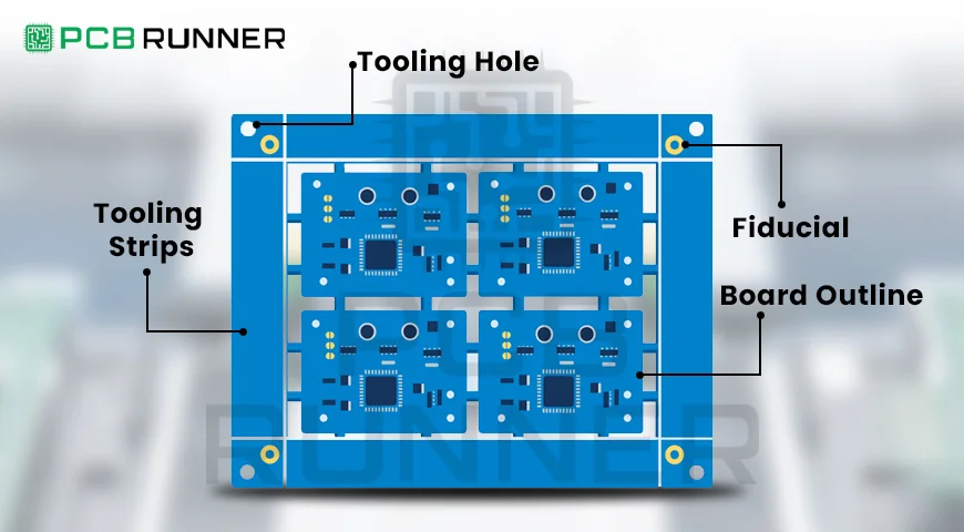
Panelization Basics
Panelization is the process of placing multiple copies of your board into one panel. The goal is to make the best use of space, simplify assembly, and reduce waste.
Here’s how you typically penalise boards:
- Determine individual board dimensions
- Add spacing between boards (usually 0.1 to 0.2 inches)
- Add tooling holes and fiducials.
- Add breakaway tabs or v-grooves to separate boards later.
Your PCB board dimensions should allow multiple boards to fit neatly inside the usable area of the standard PCB panel size. This helps keep the manufacturing cost-effective and straightforward.
Tips for Efficient Panel Design
To make sure you get the most out of your panel, follow these design tips:
1. Stick to standard dimensions
Stick to standard panel sizes unless your project requires something special. Custom sizes can slow down production and increase costs.
2. Leave enough spacing
Space between boards is needed for routing, panelling, and handling. Too little space increases the risk of damage.
3. Optimise board orientation
Some boards can be rotated to fit more units in a panel. Your PCB fabrication partner can help with this layout trick.
4. Group small boards
If your boards are tiny, consider grouping them into an array to speed up assembly and testing.
What About High-Density Interconnect (HDI) PCBs?
High-density interconnect (HDI) boards are smaller and more complex. To save space, they use micro vias, thinner traces, and more layers. While this means better performance, it also means tighter controls on board dimensions and panel layout.
Some points to consider:
- HDI boards may need tighter spacing rules
- Panels need more precise alignment.
- Standard panel sizes are still used, but yield may be lower.
Work with an experienced HDI PCB manufacturer who understands how to handle HDI designs during panelization and fabrication.
How PCB Manufacturers Handle Custom Boards
Sometimes, your board shape or size doesn’t fit the standard format. That’s okay. Custom boards are common. However, they take more planning. Most pc board manufacturers will suggest:
- Using a custom panel size
- Including extra material for support
- Designing break-off tabs carefully to avoid damage
When working with custom printed circuit board layouts, early communication with your PCB fabrication shop can help avoid problems later.
What You Should Ask Your Manufacturer
When choosing from PCB circuit board manufacturers, make sure to ask:
- What panel sizes do you support?
- What is your usable area on the panel?
- How do you handle odd-shaped boards?
- Can you help with panelisation planning?
- What are your limits for high-density interconnect boards?
These questions will help you make the right choice and avoid delays.
Final Thoughts
Choosing the correct PCB board dimensions and panel size might not sound exciting, but it’s a key part of reliable and cost-effective production. Whether you’re making standard boards or working with high-density interconnect, good planning at this stage will save time and money later.
By working with trusted PC board manufacturers and using smart design practices, you can get better-quality boards, faster turnaround, and lower costs.
Key Takeaways
- The most common standard PCB panel size is 18 x 24 inches.
- The usable area is less than the whole panel due to spacing and tooling holes.
- Good penalisation reduces waste and cost.
- Work with your PCB fabrication partner early to plan the layout.
- Custom boards may need extra care but are manageable.
- HDI boards require tight spacing and experienced handling
FAQs
Q: What is the typical spacing between boards in a panel?
A: Usually 0.1 to 0.2 inches, but it depends on routing and depaneling method.
Q: Can I use non-rectangular board shapes?
A: Yes, but they reduce panel efficiency and increase cost. Grouping or rotating may help.
Q: Are there special rules for HDI PCBs in panels?
A: Yes. HDI boards use tighter tolerances and may need extra alignment during fabrication.
Q: Who should plan the panel layout?
A: Your PCB circuit board manufacturer often handles this, but it’s best to collaborate early.
Q: How many boards fit on one panel?
A: It depends on the PCB board dimensions and how well they fit the usable area. A manufacturer can calculate this for you.

