Printed circuit boards (PCBs) are at the heart of every electronic device, from smartphones to satellites. As technology races ahead, the way we design and build PCBs is changing fast. The future is all about smart innovations, new materials, advanced machines, and clever software. In this blog, we’ll explore how the PCB fabrication process is evolving, especially in the UK, and what it means for businesses and engineers everywhere.
The Evolution of PCB Fabrication
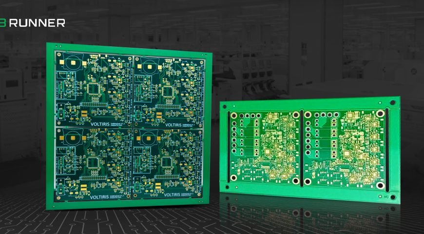
PCB fabrication has come a long way, from simple single-layer boards to today’s complex, multi-layered designs. Modern PCB fabrication UK combines precision, speed, and creativity like never before.
What Is PCB Fabrication?
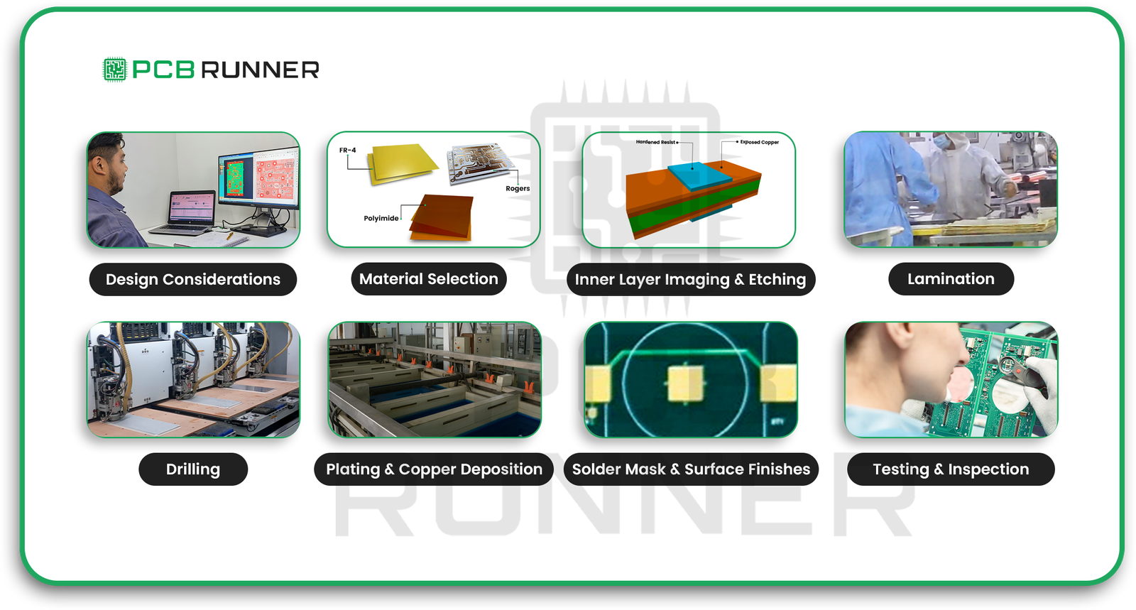
PCB fabrication is the process of making the physical board that holds and connects all the electronic parts. This includes choosing the right PCB circuit board material, layering, etching, drilling, and finishing the board so it’s ready for assembly.
Advanced Materials, The New Building Blocks
The material of PCB is more important than ever. Today’s devices need boards that are strong, light, and can handle high speeds and heat. That’s why the choice of PCB board material is a big deal in modern PCB board fabrication.
Key Innovations in PCB Board Material
- High-Performance Substrates: New substrates offer better heat resistance and electrical performance, perfect for 5G and high-speed devices1.
- Conductive Inks: Used in additive manufacturing and 3D printing, these inks allow for more flexible and custom designs.
- Biodegradable and Eco-Friendly Materials: These help reduce electronic waste and meet strict environmental rules.
Automation and AI, Smarter, Faster, Better
One of the most significant changes in PCB fabrication and assembly is the rise of automation and artificial intelligence (AI).
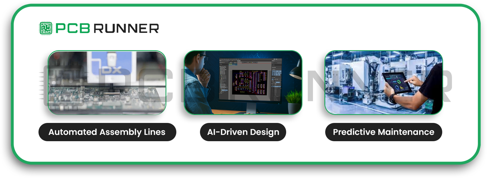
How Automation Is Changing PCB Fabrication UK
- Automated Assembly Lines: Robots now handle soldering, component placement, and even inspection, making the process faster and more accurate.
- AI-Driven Design: AI software helps design PCBs, optimizing layouts, checking for errors, and predicting failures before they happen.
- Predictive Maintenance: AI keeps machines running smoothly by spotting problems before they cause downtime.
These smart-systems mean fewer mistakes, lower costs, and higher quality boards.
3D Printing, A Game Changer for PCB Board Fabrication
3D printing isn’t just for plastic toys, it’s transforming how we make PCBs. With 3D printing, manufacturers can create complex shapes and custom boards quickly and with less waste.
Benefits of 3D Printed PCBs
- Faster Prototyping: Engineers can test ideas in days, not weeks.
- Customization: Each board can be made to fit special needs, great for aerospace or medical devices.
- Cost Savings: Less material is wasted, and there’s no need for expensive moulds or tools.
Miniaturization and HDI, Packing More Into Less
As devices get smaller, PCBs must do more in less space. This is where High-Density Interconnect (HDI) technology comes in. HDI boards use tiny holes (microvias) and thin layers to fit more connections and parts into a smaller area.
Why HDI Matters
- Supports Smaller Devices: Perfect for wearables, smartphones, and IoT gadgets.
- Improved Performance: Better signal quality and less interference.
- Greater Reliability: Fewer problems with heat and stress.
Eco-Friendly PCB Fabrication, Greener Boards for a Better Future
Sustainability is a big trend in PCB fabrication UK. Companies are looking for ways to make boards that are safer for people and the planet.
Green Innovations in PCB Board Material
- Lead-Free and Halogen-Free Boards: Safer for workers and the environment.
- Recyclable and Biodegradable Materials: Boards that break down or can be reused.
- Energy-Efficient Production: Using less power and water and recycling waste.
Smart Testing and Quality Control
Making sure every board works perfectly is critical, especially for things like medical devices or aeroplanes. New testing methods use AI, robots, and real-time sensors to catch problems early and keep quality high.
Advanced Quality Control Methods
- Automated Optical Inspection (AOI): Cameras and AI check every board for defects.
- X-Ray Inspection: Finds hidden problems inside the board5.
- IoT-Enabled Sensors: Monitor the process and alert teams if something goes wrong.
Embedded Components, The Next Step in PCB Assembly UK
Instead of placing all parts on the surface, new boards embed components inside the layers. This saves space, improves performance, and protects sensitive parts from damage.
Advantages of Embedded Components
- Smaller, Lighter Boards: Perfect for drones, satellites, and medical implants.
- Better Electrical Performance: Shorter paths mean faster signals and less noise.
- More Durable: Components are shielded from shocks and moisture.
The Role of PCB Printed Circuit Board Assembly
After fabrication, the next step is pcb printed circuit board assembly. This is where all the chips, resistors, and other parts are added to the board. Smart machines and AI make this step faster and more reliable than ever.
Key Trends in PCB Assembly UK
- Robotic Soldering: Ensures perfect joints every time.
- Automated Placement: Tiny parts are placed with pinpoint accuracy.
- Real-Time Quality Checks: Problems are caught and fixed on the spot.
Key Takeaways, Why Smart Innovations Matter
- Automation and AI are making PCB fabrication and assembly faster, cheaper, and more reliable.
- Advanced PCB board material choices mean better performance and greener electronics.
- 3D printing and embedded components are opening new doors for design and miniaturization.
- Quality control is more intelligent than ever, thanks to AI and real-time sensors.
- The UK is at the forefront of these innovations, leading the way in innovative, sustainable PCB manufacturing.
Conclusion: The Future Is Now
The world of PCB fabrication in the UK is changing fast. Smart innovations, from new materials to AI-powered machines, are making boards smaller, faster, and greener. Whether you’re an engineer, a business owner, or just a tech fan, these changes mean better, more reliable electronics for everyone.
Ready to see what innovative PCB fabrication can do for your next project? The future is here, and it’s built on smarter boards.
FAQs, Your Questions About PCB Fabrication and Assembly
Q1: What is the most common PCB board material?
FR4, a type of fibreglass epoxy, is still the most common, but new materials like ceramics and biodegradable substrates are gaining ground.
Q2: How does AI help in PCB fabrication?
AI speeds up design, catches mistakes, and predicts failures before they happen, making the whole process smarter and more reliable.
Q3: Is 3D printing used for mass production of PCBs?
Right now, it’s mainly used for prototypes and small batches, but as the technology improves, it could become common for larger runs, too.
Q4: Why are eco-friendly materials necessary in PCB fabrication?
They help reduce toxic waste, protect workers, and meet strict environmental laws, making electronics safer for everyone.
Q5: What are the benefits of embedded components in PCBs?
They save space, improve performance, and protect sensitive parts from damage.