Printed circuit boards (PCBs) are the heart of modern electronics. From the first radios to today’s smart devices, PCBs have shaped how we live and work. In this blog, we’ll take you on a journey through the history of PCB design, explore today’s best practices, and look ahead at the future of PCB manufacture. Whether you’re curious about how to design PCB board layouts or want to know what’s next for the industry, this guide is for you.
The Early Days: How PCB Design Began
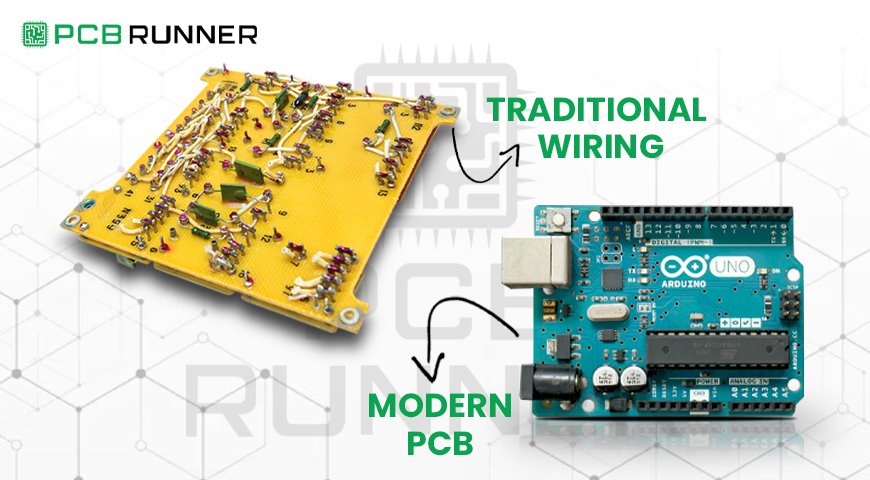
In the early days, PCBs were simple. They had just one layer and a few components. Designers drew circuits by hand, and PCB printing was a slow process. Most boards were large and bulky, used mainly in radios and early computers.
Key points from the past:
- Manual drawing and etching
- Single-layer boards
- Slow, careful assembly
As technology advanced, so did the need for better PCB board layout design. This led to the rise of printed circuit board manufacturers who could make more complex boards faster and more reliably.
How to Design a PCB Circuit Board: The Basics
If you want to know how to design a PCB circuit board, start with the basics. The steps are much easier today, thanks to modern tools and guides.
Step-by-Step PCB Design Guide
- Define Your Goals: Know what your board needs to do. List all features and connections.
- Draw a Schematic: Use software to create a diagram of your circuit.
- Select Components: Choose the right parts for your design.
- Create the Layout: Arrange components on the board for the best performance.
- Route the Traces: Connect everything with copper lines.
- Check for Errors: Use design tools to find and fix mistakes.
- Prepare for Manufacturing: Export design files for PCB manufacture.
- Prototype and Test: Build a sample and make sure it works as planned.
- Final Adjustments: Fix any issues found during testing.
- Mass Production: Send your design to a trusted printed circuit board manufacturer for large-scale production.
Tips for beginners:
- Start simple; use a basic pcb design guide.
- Keep traces short and direct.
- Group related parts together.
- Double-check your work before printing.
Today’s Trends in PCB Board Layout Design
Modern PCB board layout design is more advanced than ever. Here’s what’s shaping the industry right now:
Miniaturization and High-Density Interconnects (HDI)
Devices are getting smaller and smarter. To keep up, pcb printing now uses HDI technology. This means more connections in less space, better performance, and lower power use. HDI is key for smartphones, wearables, and medical devices.

Flexible and Rigid-Flex PCBs
New products need boards that can bend and twist. Flexible and rigid-flex PCBs are now common in cars, aeroplanes, and IoT devices. They fit into tight spaces and handle more stress without breaking.

Advanced Materials
PCB manufacturing is moving beyond traditional materials. Today’s boards use special plastics, graphene, and even biodegradable materials. These new options improve strength and heat resistance and are better for the environment.

3D PCB Printing
Additive manufacturing, or 3D printing, is changing how PCBs are made. It allows for fast prototyping and custom designs with less waste. This technology is beneficial for small batches and complex shapes.

Artificial Intelligence (AI) in PCB Design
AI is making a significant impact. It helps automate layout, checks for errors and even predicts problems before they happen. AI-powered tools are now part of every step, from design to quality control, making PCB manufacture faster and more reliable.
The Future of PCB Design
What’s next for PCB design? The industry is moving fast, and several trends are set to shape the future of PCB design:
- Smaller, Smarter Boards: Miniaturization will continue with even more powerful boards in smaller spaces.
- Eco-Friendly Manufacturing: More use of recyclable and non-toxic materials.
- AI-Driven Design: Smarter tools that can design, test, and optimize boards automatically.
- 3D and Additive Manufacturing: More use of 3D printing for both prototypes and final products.
- Flexible Electronics: Boards that can stretch, bend, and even fold for new types of devices.
Why These Trends Matter
For anyone interested in how to design a PCB board or looking for a PCB design guide, understanding these trends is essential. They help you:
- Create better, more reliable products
- Reduce time and cost in development
- Stay ahead in a fast-changing market
PCB Printing: Then and Now
Here’s a quick look at how PCB printing has changed over time:
| Era | Method | Key Features | Impact on Design |
| Early Days | Manual drawing, etching | Simple, single-layer | Slow, error-prone |
| 1980s-2000s | Automated tools, CAD | Multilayer, faster | More complex designs |
| Today | HDI, flexible, 3D printing | Small, powerful, custom | Fast, efficient, precise |
| Future | AI, eco-materials, additive | Smart, green, adaptable | Smarter, sustainable |
Best Practices for Modern PCB Board Layout Design
- Plan Ahead: Define your goals and constraints early.
- Use Ground and Power Planes: This reduces noise and improves stability.
- Keep Traces Short: Shorter paths mean better performance.
- Group Components: Place related parts close together.
- Check Manufacturer Capabilities: Make sure your PCB manufacturing partner can handle your design’s complexity.
- Test Early and Often: Prototype and test before full production.
Conclusion
PCB design has come a long way, from hand-drawn layouts to AI-powered, eco-friendly boards. Whether you’re new to electronics or an experienced engineer, staying updated on trends like HDI, flexible boards, and AI-driven tools will help you succeed. If you want to learn more about how to design a PCB board or need a reliable partner for PCB manufacture, keep exploring and stay ahead of the curve.
Ready to design your next PCB? Stay informed, use the latest tools, and partner with trusted printed circuit board manufacturers for the best results. The future of PCB design is bright and it’s just getting started!
Frequently Asked Questions (FAQs)
Q1: How do I start designing a PCB circuit board?
Begin with a clear schematic, choose your components, and use a simple PCB design guide to lay out your board. Many free tools are available to help beginners.
Q2: What is HDI in PCB design?
HDI stands for High-Density Interconnect. It allows more connections in a smaller area, making it perfect for compact devices like smartphones and wearables.
Q3: How is 3D printing changing PCB manufacture?
3D printing allows for fast prototyping and custom designs. It reduces waste and makes it easier to create complex shapes that were not possible before.
Q4: What are the benefits of flexible PCBs?
Flexible PCBs can bend and fit into tight spaces. They are durable and ideal for products that need to move or flex, like medical devices and wearables.
Q5: What is the future of PCB design?
The future of PCB design includes smarter, smaller, and more eco-friendly boards. AI and 3D printing will play a significant role, making design and manufacturing faster and more efficient.