Ensuring high-quality PCB assembly is crucial for the reliability and performance of electronic devices. Any defect in the assembly process can lead to malfunctions, failures, or costly rework. This is why PCB assemblers rely on a range of inspection techniques to detect issues early and maintain high manufacturing standards.
From automated optical inspection (AOI) to manual visual checks, these methods help PCB fabrication facilities identify soldering defects, misaligned components, and electrical faults before final deployment. In this guide, we will explore the most effective circuit board assembly inspection techniques and how they improve overall PCB quality and reliability.
Why PCB Inspection is Important?
Modern electronic devices are becoming smaller, more complex, and densely packed with components. This makes it essential for PCB assemblers to use advanced inspection methods to ensure manufacturing accuracy and defect-free production.
Inspection plays a key role in:
- Detecting soldering defects like cold joints, bridging, and insufficient solder
- Identifying misaligned or missing components
- Ensuring trace integrity to prevent electrical failures
- Reducing rework and product recalls
- Improving overall production efficiency
With multiple inspection techniques, manufacturers can maintain consistent quality while meeting industry standards for high-performance PCBs.
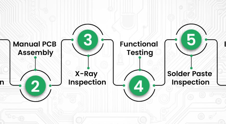
Key PCB Inspection Techniques
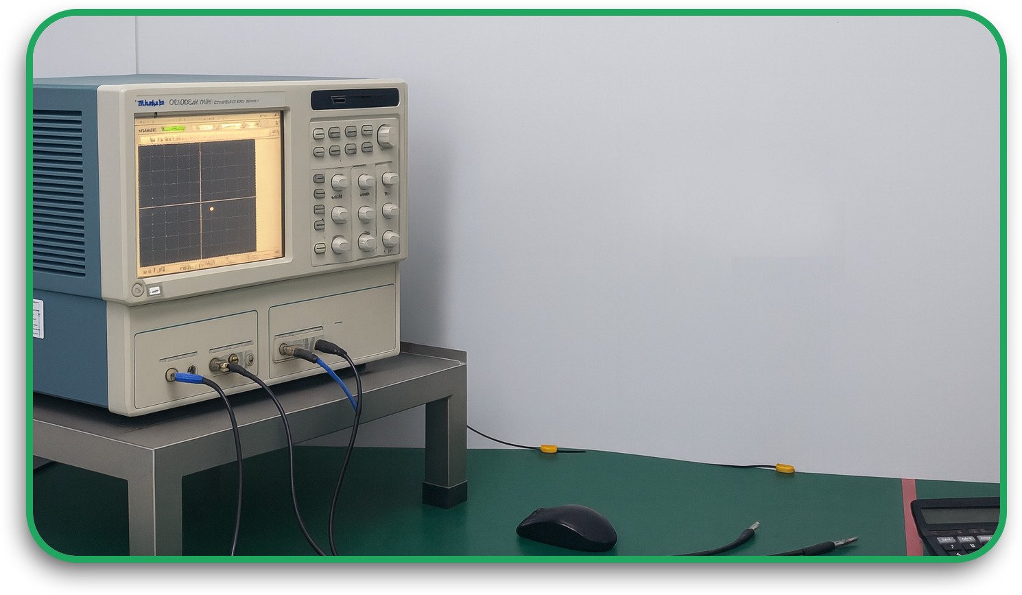
1. Automated Optical Inspection (AOI PCB Inspection)
Automated Optical Inspection (AOI) is one of the most widely used techniques in PCB fabrication. It uses high-resolution cameras and AI-driven image processing to scan boards for defects, soldering issues, and misaligned components.
Benefits of AOI in PCB Inspection:
- Fast and efficient – Scans large batches of PCBs in seconds
- High accuracy – Detects defects with precision down to micrometers
- Non-contact method – Does not risk damaging the board
- AI integration – Improves defect recognition and reduces false positives
AOI is ideal for inspecting Surface Mount Technology (SMT) boards with fine-pitch components. It ensures that every component is placed correctly and securely before moving forward in the assembly process.
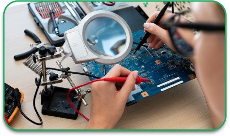
2. Manual PCB Assembly Visual Inspection
Despite advancements in automation, manual inspection remains an essential step in PCB fabrication. Skilled technicians examine boards using magnification tools, microscopes, and bright lighting to identify defects that machines might miss.
Why Manual Inspection is Important:
- Detects subtle defects such as hairline cracks or irregular solder joints
- Allows human judgment for complex PCB layouts
- Useful for low-volume production or prototype testing
While manual inspection is effective, it is time-consuming and less reliable for mass production. That’s why it is often combined with automated testing methods to ensure thorough quality checks.

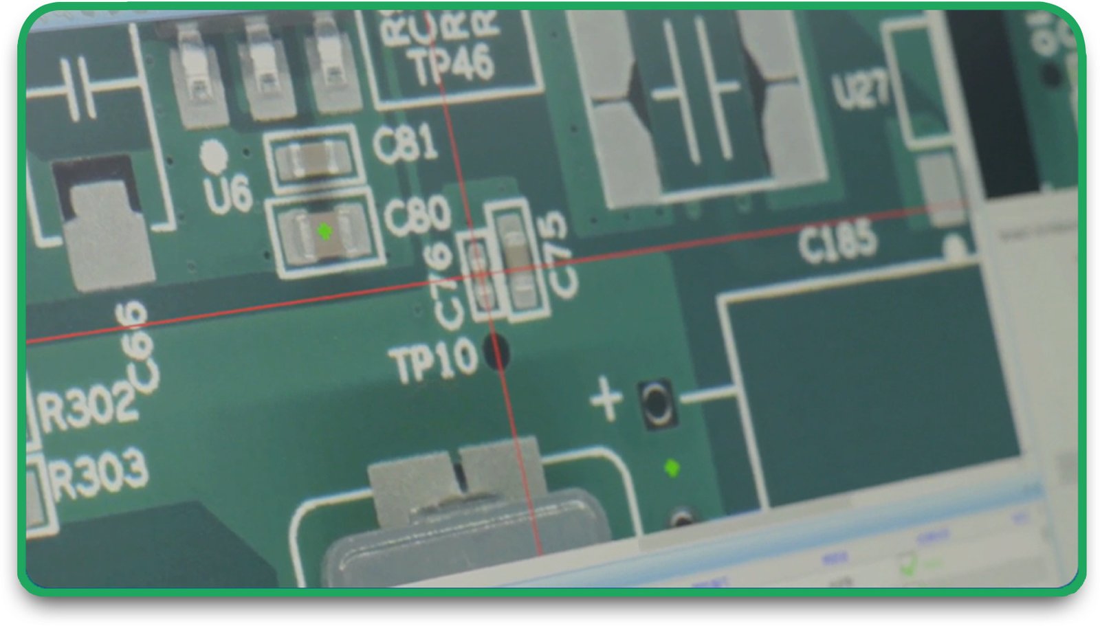
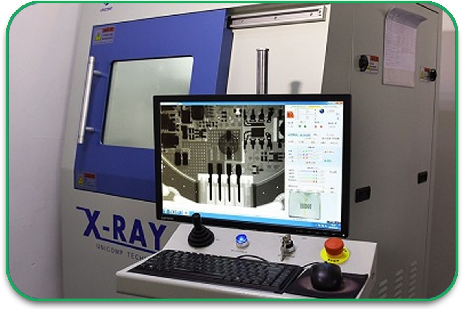
3. X-ray Inspection for Hidden Defects
For multi-layer PCBs or boards with Ball Grid Array (BGA) components, X-ray inspection is essential. This technique allows manufacturers to see through layers and inspect connections that are not visible to the naked eye.
Advantages of X-ray PCB Inspection:
- Reveals hidden solder joints and internal traces
- Detects voids, cracks, and short circuits
- Non-destructive method for detailed analysis
X-ray inspection is widely used in high-reliability applications such as aerospace, medical, and automotive electronics.
4. Functional Testing for Performance Validation
Once a PCB is assembled, it must be tested to ensure it works as intended. Functional testing involves applying power to the board and checking its response to various inputs.
Key Functional Testing Methods:
- Boundary scan testing – Used for testing digital circuits with limited physical access
- In-circuit testing (ICT) – Checks individual components and connections
- Flying probe testing – A flexible alternative to ICT for small batch testing
Functional testing is essential in verifying PCB functionality, signal integrity, and power distribution. It helps manufacturers identify faulty components or design flaws before mass production.
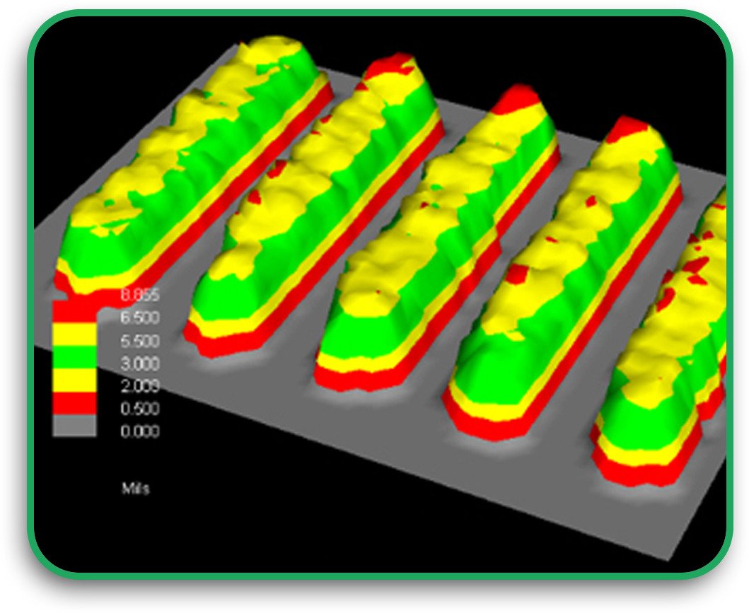
5. Solder Paste Inspection (SPI) for SMT Assembly
For Surface Mount Technology (SMT) PCBs, solder paste application is a critical step. Any issues with paste alignment, thickness, or consistency can lead to poor solder joints and defective boards.
Solder Paste Inspection (SPI) uses 3D imaging and laser scanning to analyze solder paste deposits before components are placed.
Why SPI is Important:
- Reduces soldering defects such as bridging or missing paste
- Ensures even distribution of solder paste
- Improves yield rates and reduces rework
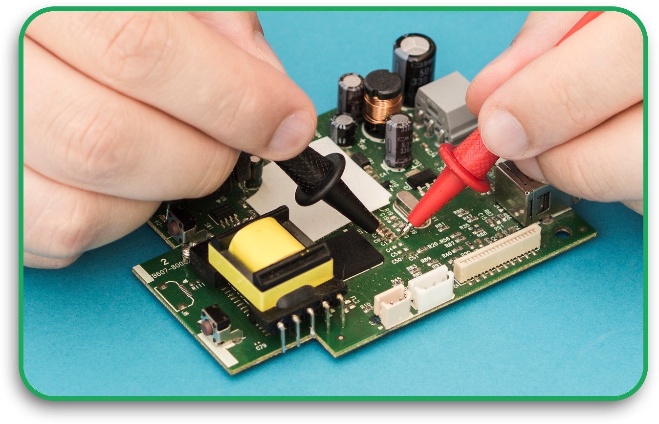
6. Electrical Testing for Short Circuits and Opens
To verify the electrical continuity of a PCB, electrical testing methods such as bed-of-nails testing or flying probe testing are used.
Key Electrical Testing Benefits:
- Identifies open circuits, short circuits, and incorrect component values
- Ensures power integrity across multiple layers
- Prevents latent failures caused by weak connections
Best Practices for High-Quality PCB Inspection
To maximize the effectiveness of inspection techniques, PCB assemblers should follow these best practices:
1. Integrate Multiple Inspection Methods
Using a combination of AOI, X-ray, functional testing, and manual inspection ensures comprehensive defect detection.
2. Implement Real-Time Quality Control
Tracking defects in real-time allows manufacturers to identify process issues early and reduce waste.
3. Use Industry Standards for PCB Inspection
Following IPC-A-610 and ISO 9001 standards ensures that PCBs meet global quality requirements.
4. Train Technicians for Manual Inspection
Even with automated tools, skilled technicians play a vital role in verifying and troubleshooting defects.
5. Optimize Design for Manufacturability (DFM)
By designing PCBs for easier assembly and inspection, manufacturers can reduce errors and improve efficiency.
Why PCB Inspection is Essential for Your Project
Investing in high-quality PCB inspection leads to:
- Better product reliability
- Fewer defects and reduced rework
- Lower production costs
- Faster time-to-market
If you need reliable PCB fabrication and assembly, partnering with an experienced PCB assembler is key.
Conclusion
PCB inspection is a critical step in ensuring high-quality circuit board assembly. From AOI PCB inspection to X-ray analysis and functional testing, manufacturers use a variety of techniques to detect defects and improve reliability.By integrating advanced inspection technologies and following best practices, PCB assemblers can deliver superior-quality products that meet industry standards.
Need High-Quality PCB Manufacturing?
At PCB Runners, we specialize in precision PCB fabrication and assembly with rigorous inspection processes to ensure flawless performance. Contact us today for a free quote and experience top-tier PCB manufacturing services.
Frequently Asked Questions (FAQs)
1. What is AOI in PCB inspection?
AOI (Automated Optical Inspection) is a non-contact inspection method that uses cameras and image processing software to detect soldering defects, missing components, and alignment issues on PCBs.
2. Why is X-ray inspection important for PCB assembly?
X-ray inspection is used to detect hidden defects such as voids, cracks, and poor solder joints, especially in multi-layer PCBs and BGAs.
3. How does functional testing improve PCB quality?
Functional testing simulates real-world operating conditions to ensure the PCB performs as expected, identifying faulty components and circuit errors.
4. What are the most common PCB defects?
Common defects include solder bridges, cold joints, missing components, short circuits, and open traces.
5. How can I ensure my PCBs are high quality?
Partnering with a trusted PCB assembler, using advanced inspection methods, and following DFM principles will ensure high-quality PCBs.