


Heavy Copper PCBs
Heavy Copper PCBs for High Current, High Power Designs
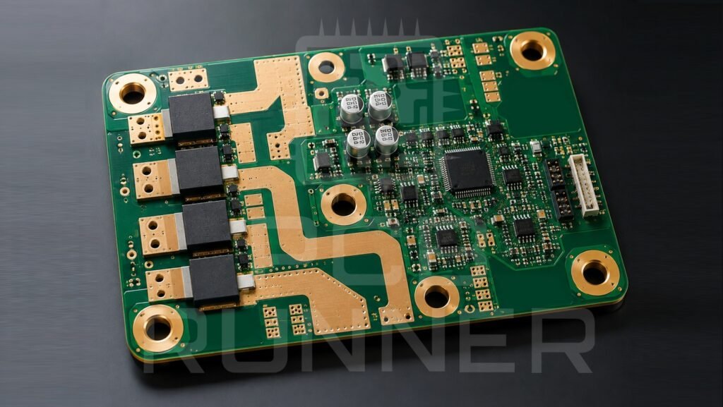
When current and power density increases, the standard copper can become a limitation. Heavy copper PCBs provide greater conductor capacity and improved heat distribution where wider traces alone are not practical, while localized copper features or busbars can support more demanding power paths.
PCB Runner manufactures heavy copper PCBs from 2 oz through 20 oz, supporting multilayer stackups, mixed copper weights and high-current designs from prototype through production.
Capability Chart
| Parameter | Specification |
|---|---|
| Copper Weight | 2 oz to 20 oz per layer, higher on request |
| Layer Count | 2 to 20 layers |
| Base Material | FR-4, high-Tg FR-4, polyimide, metal-backed laminates |
| Minimum Trace/Space | Scales with copper weight, tighter at lower oz, wider above 10 oz |
| Finished Copper Thickness | Up to 1000 microns, inner and outer layers |
| Surface Finish | ENIG, HASL, immersion silver, OSP |
| Certifications | ISO 9001, IPC Class 2, 3, and 3A, RoHS |
| Inspection | AOI, X-ray, cross-section, impedance testing |
| Prototype Lead Time | 3 to 5 working days |
Trace width and spacing tighten or loosen depending on copper weight, so the numbers above are a starting point. We confirm exact tolerances once we see your layout.
Services Offered
Heavy Copper PCB Fabrication
We fabricate boards from 2 oz through 20 oz copper using step plating to keep the etch consistent at higher weights. Thicker copper is harder to etch cleanly, and this is where most quality problems show up if a shop skips the extra plating steps.
Multilayer Heavy Copper Stack-Ups
Power converter designs usually need heavy copper for the current path and standard copper for control and signal layers on the same board. We build mixed stack-ups so you are not running two separate boards for one function.
Heavy Copper PCB Assembly
We assemble heavy copper boards in-house, including component sourcing, SMT and through-hole placement, and functional test. Heavy copper boards are thicker and heavier than standard PCBs, so reflow profiles and fixture design need adjusting, which we handle as part of the build.
Copper Coin and Custom Copper Thickness
Some designs only need extreme current handling in one small area of the board rather than across the whole layer. Our Copper Coin Technologyand copper thickness and trace width options solve that without overbuilding the rest of the board.
Prototype Through Production
The same tooling and inspection process runs from your first prototype heavy copper PCB through to volume production, so nothing changes when you move from testing to a real order.
Why Choose PCB Runner
A board that looks right on the shop floor is not the same as a board that works right in the field. The difference usually comes down to how the assembly process is run.
Own our manufacturing floor
Free engineering review before fabrication starts.
Supplied PCBs across the UK and Europe
- We own our manufacturing floor. Your thick copper PCB board is built and inspected on our line, not handed off to a broker we do not control.
- Every order gets a free engineering review before fabrication starts. Our CAM team checks copper callouts, stack-up, and drill data against your Gerber files and flags anything that would cause a problem later.
- Call us and a person picks up, not a support ticket. Heavy copper projects often come with tight deadlines, and getting a straight answer on lead time or plating tolerance matters more than a fast automated reply.
- We have supplied PCBs across the UK and Europe for over 10 years, and a large share of our new orders come from existing customers referring to us.
Quality & Inspection
Assembly defects are often smaller and harder to catch than fabrication defects, since a lot of what goes wrong happens underneath a component rather than on the surface. That is why inspection at this stage has to be layered, not left to a single check at the end.
Automated Optical Inspection (AOI)
Automated Optical Inspection runs on every panel to catch trace and pad defects before the board moves to the next process step..
X-Ray Inspection
X-ray inspection checks via fill and copper plating, which is where heavy copper boards are more prone to defects than standard weight boards.
Cross-section analysis
Cross-section analysis confirms the finished copper thickness matches what was specified, not just what the plating log shows.
Impedance testing
Impedance testing runs on any board where controlled impedance layers sit alongside heavy copper planes.
ISO 9001 certification
We hold ISO 9001 certification and qualify to IPC Class 2, Class 3, and 3A depending on what your application needs. All material is RoHS compliant and traceable back to the lot.
Industries We Support
Assembly requirements shift a lot depending on where the board ends up. Here is where our assembly capabilities get used most often.
Power Electronics
Power supplies and DC-DC converters use heavy copper to carry current without the trace overheating.
Automotive and EV
Battery management systems and charging modules use heavy copper to hold up under sustained current and vibration.
Renewable Energy
Solar inverters use thick copper PCB board designs to manage current through the DC to AC conversion stage.
Industrial Automation
Motor drives and welding equipment need heavy copper to run continuously at high current without failing.
Aerospace and Defense
Heavy copper adds mechanical strength and thermal margin where a board cannot be allowed to fail in the field.
Telecommunications
Base station power supplies use heavy copper to manage current density inside a compact enclosure.
Medical Equipment
Devices that draw significant current benefit from the added thermal stability heavy copper provides.
A medical board and an automotive board can look similar on paper but need very different assembly considerations once you factor in how and where they will actually be used. We adjust the process to the application rather than running every job the same way.
Frequently Asked Questions
A heavy copper PCB is a circuit board with copper weight of 2 oz per square foot or more on its layers, compared to the 0.5 oz to 1 oz used on standard boards. The extra copper carries more current and spreads heat more effectively.
There is no technical difference. Thick copper PCB and heavy copper PCB describe the same thing, and both terms are used interchangeably across the industry.
We manufacture heavy copper PCBs from 2 oz up to 20 oz per layer as standard. Higher weights can be quoted depending on your stack-up and application.
1 oz copper works out to roughly 35 microns, or 1.4 mil, of copper thickness per square foot. Heavy copper boards start well above this, typically from 2 oz upward.
We do not enforce a minimum order quantity on heavy copper PCBs. We quote single prototypes the same way we quote production volume.
Most heavy copper prototypes ship in 3 to 5 working days. Higher copper weights and more layers can add a day or two depending on the stack-up.
Send Gerber RS-274X files, your stack-up with copper weight per layer, drill files, and any notes on trace width, spacing, or impedance. For assembly, include a BOM and X and Y placement data as well.
Heavy copper PCBs are used in power supplies, EV battery and charging systems, solar inverters, motor drives, welding equipment, and any design where a trace needs to carry more current than standard copper can handle safely.
Ready to Build Your Heavy Copper PCB?
Send us your Gerber files and stack-up and we will review your heavy copper PCB design before quoting. Whether it is one prototype board or a production run, we fabricate and assemble it under one roof.



