


What Is a High Frequency PCB?
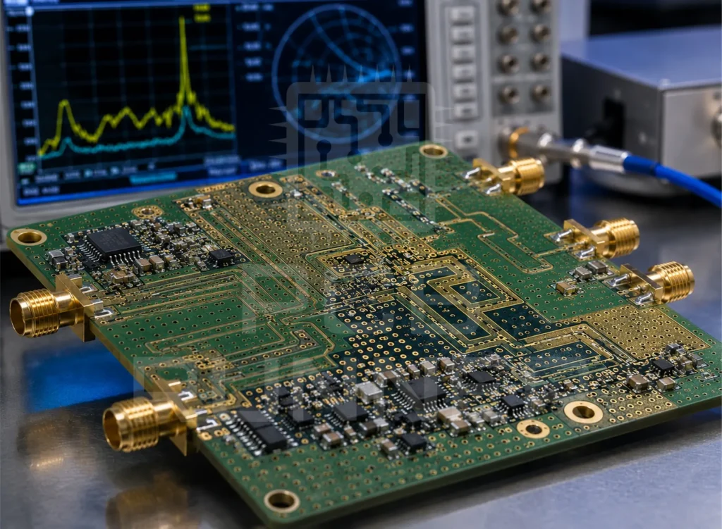
A high frequency PCB is a circuit board built with a substrate designed to carry signals above roughly 500 MHz without the loss, drift, or heat problems that show up on standard FR-4. Above that range, the dielectric constant and loss tangent of the material start to shape how well your signal actually gets from A to B.
That’s why RF and microwave designs use laminates like Rogers RO4000 series, PTFE, or ceramic-filled materials instead of ordinary epoxy glass. These substrates hold their electrical properties steady across temperature and frequency, which is exactly what you need for radar, wireless infrastructure, and high-speed data links.
Get the material choice wrong and no amount of clever layout will fix it. Get it right, and the board performs the way your simulation predicted.
Why Work With Us
Material expertise, not guesswork
We've fabricated boards across the full range of Rogers and PTFE laminates and know how each one behaves in production, not just on a datasheet.
Impedance verified, every panel
Test coupons are built into the panel and measured before boards ship, so the number on your drawing matches the number on your board.
Hybrid stack-ups done properly
RF material only where the signal needs it, FR-4 everywhere else. That keeps cost down without touching performance where it counts.
Engineers review your files, not a checklist
Every Gerber and stack-up goes past someone who has actually routed high frequency layouts before.
No minimum order
One prototype or a production run, same review process either way.
Fast turnaround on quotes
You get pricing and lead time back the same day, so material selection doesn't stall your schedule.
Features & Manufacturing Capabilities
Our capabilities include:
Rogers RO3000, RO4000, and RT/duroid laminates
PTFE and ceramic-filled high frequency substrates
Hybrid Rogers-FR4 and PTFE-FR4 stack-ups
Single-layer through high-layer-count multilayer construction
Controlled impedance to tight tolerance, verified on test coupons
Blind, buried, and laser-drilled microvias for compact RF layouts
Edge plating and castellated holes for shielding and module mounting
ENIG, ENEPIG, and immersion silver finishes suited to RF performance
Support for frequencies from a few hundred MHz through mmWave
Our High Frequency PCB Manufacturing Process
01
Submit Your Files
Send Gerbers, stack-up requirements, and target impedance values. Tell us the operating frequency; it changes the material recommendation.
02
Material and Design Review
Our engineers check the stack-up against your frequency and impedance targets and flag anything that won't hold up in fabrication.
03
Quote and Approval
You get a quote with lead time and confirmed material. Production starts once you sign off.
04
Fabrication
Boards are built to the approved stack-up, with impedance-controlled layers etched and tested on integrated coupons.
05
Testing and Delivery
Every panel is impedance-tested, inspected, and electrically verified before it ships.
Technical Specifications
| Specification | Detail |
|---|---|
| Layer Count | Single-layer to upto 50 layers multilayer |
| Base Materials | Rogers RO3000/RO4000 series, RT/duroid, PTFE, Megtron 6,7,8, Nelco, Arlon, Isola 370HR, FR408HR and more. |
| Dielectric Constant (Dk) | 2.2 to 10.2 depending on material |
| Standard Trace Width/Spacing | 4 mil and 2mil on critical locations |
| Finish Via Hole Diameter | 6 mil and below, laser microvias available |
| Copper Thickness | 0.5 oz to 12 oz |
| Impedance Tolerance | ±10% & ±5% for tighter on request |
| Surface Finishes | ENIG, ENEPIG, Hard gold, soft gold, immersion silver, immersion tin |
If your design needs a material or tolerance outside this range, talk to us before you finalize the stack-up. It’s cheaper to change a layer count on paper than after fabrication.
Standards & Quality Assurance
ISO 9001:2015
IPC Class 2 & 3
AOI
RoHS Compliant
X-ray inspection
Our Quality Process includes:
- ISO 9001:2015 certified manufacturing
- IPC Class 2 and Class 3 build standards
- RoHS-compliant materials across all laminate options
- Impedance verification via integrated test coupons on every panel
- X-ray inspection for buried vias and hidden connections
- Electrical testing for continuity and isolation before shipment
- Micro-sectioning available on request for critical builds
Applications & Industries
Automotive
Radar sensors, ADAS modules, V2X communication
Telecommunications
5G infrastructure, base stations, antenna arrays
Aerospace & Defence
Radar systems, satellite communication, EW systems
Medical
Imaging equipment, wireless diagnostic devices
Industrial
Sensor networks, wireless control systems
Semi Conductor industry
Lithography systems equipment boards, controller cards, Load Boards, Semiconductor testing boards, FPGA boards
Prototype to Production
A high frequency board that performs well as a prototype needs to perform the same way at volume. Material behavior, impedance, and layer registration all have to stay consistent as quantities scale.
| Stage | What We Do |
|---|---|
| Prototype | Build and test small batches to confirm electrical performance |
| Design Review | Refine stack-up and layout based on prototype results |
| Pilot Run | Validate the process at low volume before committing to full production |
| Volume Production | Scale using the same approved stack-up and test coupons |
Because the same engineering team and materials carry through every stage, moving from prototype to production doesn’t mean starting the review process over.
Frequently Asked Questions
We build boards for applications from a few hundred MHz up to 77 GHz, depending on material and stack-up.
Below a few hundred MHz, FR-4 is usually fine. Above that, loss and impedance drift start to matter, and a hybrid or full Rogers stack-up is worth the cost.
Yes. Hybrid stack-ups put RF material only where the signal path needs it, which keeps cost down.
We build test coupons into the production panel and measure them before boards ship, so you get a report against the same panel your boards came from.
No. We run the same review and test process whether you order one board or a production batch.
Gerber files, your target stack-up or impedance values, and operating frequency. A BOM and pick-and-place file if assembly is included.
Ready to Build Your High Frequency PCB?
Every order gets a stack-up and impedance review from an engineer before fabrication starts, so problems get caught on paper, not on a finished board.
Request a quote today and talk to our team about material selection before you lock in your design.



